ATTENTION: Due to increased demand and order volume, processing time may take an additional 1-3 business days.
HomeCommunitySubject2N1711 NPN Power Transistor: 2N1711 Transistor Datasheet, Pinout and Equivalents

2N1711 NPN Power Transistor: 2N1711 Transistor Datasheet, Pinout and Equivalents

Transistors - Bipolar (BJT) - Single Bipolar Transistors - BJT NPN General Purpose The 2N1711 is silicon Planar Epitaxial NPN transistor in Jedec TO-39 metal case.

408

Nov 9, 2021

Tess Morley

EQD Dirt Transmitter/Fuzz Face Hybrid 2N1711 Transistors

Transistors - Bipolar (BJT) - Single Bipolar Transistors - BJT NPN General Purpose

The 2N1711 is silicon Planar Epitaxial NPN transistor in Jedec TO-39 metal case. It is intended for use in high-performance amplifiers, oscillators, and switching circuits. This article is going to introduce the 2N1711 transistor.
2N1711

5600In Stock
Min.: 1 Mult.: 1
Price not displayed? Not available to buy online? Please send an RFQ, and we will respond immediately.
Quick Links

What is 2N1711?

The 2N1711 is a metal case NPN transistor with a TO-39 package. The transistor's main functions include switching, amplification, and oscillator. It can deliver 500mA of collector current when used as a switch. The transistor's peak collector current can reach 1A. The greatest collector current a transistor can drive in a microsecond and millisecond pulses are determined by the peak collector current value.

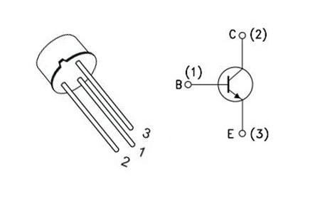
2N1711 Pinout

Specifications

2N1711 Tech Specifications

STMicroelectronics 2N1711 technical specifications, attributes, parameters and parts with similar specifications to STMicroelectronics 2N1711.

Product Attribute Attribute Value
MountThrough Hole
Mounting TypeThrough Hole
Package / CaseTO-205AD, TO-39-3 Metal Can
Number of Pins3Pins
Weight4.535924g
Transistor Element MaterialSILICON
Collector-Emitter Breakdown Voltage50V
Collector-Emitter Saturation Voltage500mV
Number of Elements1 Element
hFEMin40
Operating Temperature175°C TJ
PackagingTube
JESD-609 Codee3
Pbfree Codeyes
Part StatusObsolete
Moisture Sensitivity Level (MSL)1 (Unlimited)
Product Attribute Attribute Value
Number of Terminations3Terminations
Terminal FinishMatte Tin (Sn)
Voltage - Rated DC75V
Max Power Dissipation800mW
Terminal PositionBOTTOM
Terminal FormWIRE
Current Rating500mA
Frequency100MHz
Base Part Number2N17
Pin Count3
Element ConfigurationSingle
Power Dissipation800mW
Transistor ApplicationSWITCHING
Gain Bandwidth Product100MHz
Polarity/Channel TypeNPN
Transistor TypeNPN
Product Attribute Attribute Value
Collector Emitter Voltage (VCEO)50V
Max Collector Current500mA
DC Current Gain (hFE) (Min) @ Ic, Vce35 @ 100mA 10V
Current - Collector Cutoff (Max)10nA ICBO
Vce Saturation (Max) @ Ib, Ic1.5V @ 15mA, 150mA
Transition Frequency100MHz
Collector Base Voltage (VCBO)75V
Emitter Base Voltage (VEBO)7V
Height6.6mm
Length9.4mm
Width9.4mm
Radiation HardeningNo
RoHS StatusROHS3 Compliant
Lead FreeLead Free
0 Products View Similar

2N1711 Features

  • Package Type: TO-39

  • Transistor Type: NPN

  • Max Collector Current(IC): 500mA

  • Max Collector-Emitter Voltage (VCE): 50V

  • Max Collector-Base Voltage (VCB): 75V

  • Max Emitter-Base Voltage (VBE): 7V

  • Max Collector Dissipation (Pc): 800 Milliwatt

  • Max Transition Frequency (fT): 100 MHz

  • Minimum & Maximum DC Current Gain (hFE): 100 to 300

  • Max Storage, Operating & Junction temperature range: -65 to 200 Centigrade

2N1711 Benefits

  • High breakdown voltage,

  • Low leakage current,

  • Low capacity

  • Beta useful over an extremely wide current range


2N1711 Applications

  • Switching applications

  • Audio Amplification Circuits

  • Audio Pre amplification Circuits

  • RF applications

  • Any signal amplification


2N1711 Equivalents

2N4032, 2N1711A, 2N3107, 2N3019

Where and How to Use 2N1711?

The 2N1711 transistor is suitable for a wide range of applications. As previously stated, it can be used as a switch and can drive loads up to 500mA. It may also be used as an amplifier, allowing it to amplify a wide range of signals. It can also be employed in radio frequency applications with a frequency range of fewer than 100 MHz.


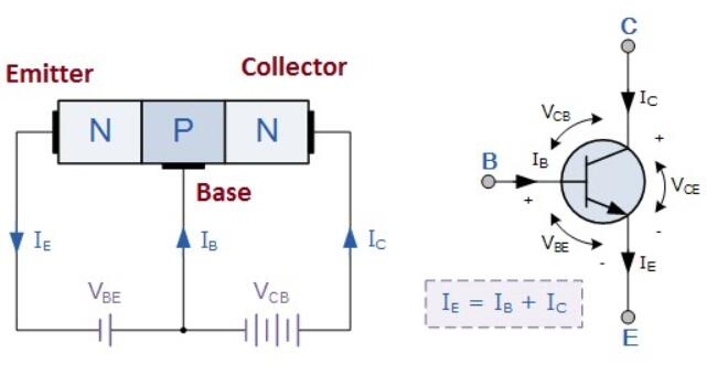
How does 2N1711 work in a circuit?

2N1711 Circuit

  • The common base, common emitter, and common collector configurations are the three main configurations for this NPN transistor.

  • Because it has the requisite voltage and power gain for amplification, the common-emitter arrangement is extensively utilized for amplification.

  • The input signal can be increased by 20dB, which is roughly 100 times more than the input signal.

  • The collector voltage is higher than the base voltage, which is vital to remember.

  • On the emitter side, the current is a mixture of base and collector currents.

  • The size and doping concentration of emitter and collector are the primary differences. The collector has a low doping level, but the emitter has a high doping level.

  • The base currency in this transistor is always the smallest, whereas the emitter current is always the biggest.

  • The forward current gain of the transistor is represented by beta β. It is an amplification factor, the value at which the current is being amplified. It is the ratio between collector current the base current. As it is a ratio between two currents so it features no unit.

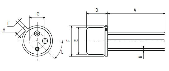
2N1711 Dimensions

2N1711 Dimensions

2N1711 Manufacturer

STMicroelectronics is a global independent semiconductor company and is a leader in developing and delivering semiconductor solutions across the spectrum of microelectronics applications. An unrivaled combination of silicon and system expertise, manufacturing strength, Intellectual Property (IP) portfolio, and strategic partners positions the Company at the forefront of System-on-Chip (SoC) technology, and its products play a key role in enabling today's convergence trends.


Datasheet PDF

Download datasheets and manufacturer documentation for STMicroelectronics 2N1711.

2N1711 Documents

Download datasheets and manufacturer documentation for 2N1711

Frequently Asked Questions

What is the use of 2N1711?
The 2N1711 is a silicon Planar Epitaxial NPN transistor in Jedec TO-39 metal case. It is intended for use in high-performance amplifiers, oscillators,s, and switching circuits. The 2N1711 is also used to advantage in amplifiers where low noise is an important factor.
How does 2n1711 work?
2n1711 is a bipolar device where conduction is carried out by the movement of both charge carriers holes and electrons. When we apply positive voltage at the base side, it gets biased and allows controlling large current at the emitter and collector side.
FAQ
What is the use of 2N1711?
The 2N1711 is a silicon Planar Epitaxial NPN transistor in Jedec TO-39 metal case. It is intended for use in high-performance amplifiers, oscillators,s, and switching circuits. The 2N1711 is also used to advantage in amplifiers where low noise is an important factor.
How does 2n1711 work?
2n1711 is a bipolar device where conduction is carried out by the movement of both charge carriers holes and electrons. When we apply positive voltage at the base side, it gets biased and allows controlling large current at the emitter and collector side.

TAGS

Share