ATTENTION: Due to increased demand and order volume, processing time may take an additional 1-3 business days.
HomeCommunitySubject2SC1815 NPN-Transistor : Pinout, Equivalents and Datasheet

2SC1815 NPN-Transistor : Pinout, Equivalents and Datasheet

Hello everyone, I am Rose. Today I will introduce 2SC1815 to you. The 2SC1815 is a 50V 150mA general purpose NPN low-power silicon transistor with a maximum gain value of 700. This article mainly introduces pinout, equivalents, datasheet, and other detailed information about Central Semiconductor 2SC1815.

2153

Sep 10, 2021

Roxanne Ellis

High volt shock by transistor 2SC1815


Hello everyone, I am Rose. Today I will introduce 2SC1815 to you. The 2SC1815 is a 50V 150mA general purpose NPN low-power silicon transistor with a maximum gain value of 700. This article mainly introduces pinout, equivalents, datasheet, and other detailed information about Central Semiconductor 2SC1815.

2SC1815

32In Stock
Min.: 1 Mult.: 1
Price not displayed? Not available to buy online? Please send an RFQ, and we will respond immediately.
Quick Links

2SC1815 Description

The 2SC1815 is a 50V 150mA general purpose NPN low-power silicon transistor with a maximum gain value of 700.  It is produced by Central Semiconductor. The tube withstand voltage is 40V, Pcm=400mW, Icm=150mA, and it adopts TO-92 package. The transistor polarity is NPN. This makes the transistor suitable for amplifier applications.


2SC1815 Pinout

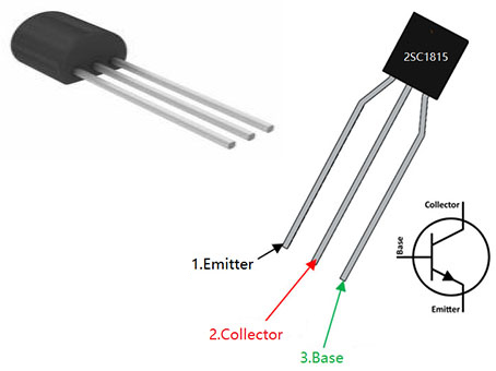
2SC1815 Pinout


Pin Number Pin Name Description
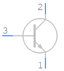
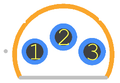
1 Emitter Current Drains out through emitter, normally connected to ground
2 Collector Current flows in through collector, normally connected to load
3 Base Controls the biasing of the transistor, Used to turn ON or OFF the transistor

2SC1815 Pin Description

2SC1815 CAD Model

Symbol

Footprint

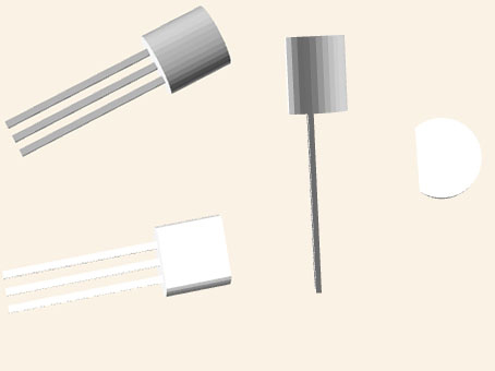
3D Model

2SC1815 Features

●General Purpose NPN Transistor

●DC Current Gain (hFE) 70 to 700

●Continuous Collector current (IC) is 150mA

●Collector-Emitter voltage (VCE) is 50V

●Collector-Base voltage (VCB) is 60V

●Emitter-base breakdown voltage (VEBO): 5V

●Collector-emitter saturation voltage drop (VCE): 0.25V

●Transition Frequency: 80MHz

●Base current (IB): 50mA

●Power dissipation (PC): 400mW

●Available in To-92 Package

Specifications

Central Semiconductor 2SC1815 technical specifications, attributes, parameters and parts with similar specifications to Central Semiconductor 2SC1815.

2SC1815 Tech Specifications

Central Semiconductor 2SC1815 technical specifications, attributes, parameters and parts with similar specifications to Central Semiconductor 2SC1815.

Product Attribute Attribute Value
Factory Lead Time8 Weeks
Surface MountNO
Transistor Element MaterialSILICON
Collector-Emitter Breakdown Voltage50V
Number of Elements1 Element
Power Dissipation (Max)400mW
Published2016
Part StatusActive
Product Attribute Attribute Value
Number of Terminations3Terminations
ECCN CodeEAR99
Terminal PositionBOTTOM
Terminal FormTHROUGH-HOLE
JESD-30 CodeO-PBCY-T3
ConfigurationSINGLE
Transistor ApplicationAMPLIFIER
Polarity/Channel TypeNPN
Product Attribute Attribute Value
Collector Emitter Voltage (VCEO)250mV
Max Collector Current150mA
JEDEC-95 CodeTO-92
Transition Frequency80MHz
Frequency - Transition80MHz
DC Current Gain-Min (hFE)70
RoHS StatusRoHS Compliant
0 Products View Similar

Where to use 2SC1815?

The 2SC1815 is a general-purpose NPN transistor that is commonly used in Amplifier applications. There are four variants, the 2SC1815O will have a gain value of 70 to 140 and the 2SC1815Y will have 1020 to 240, the 2SC1815GR will have 200 to 400 and the 2SC1815L will have a gain range from 350 to 700.


This NPN transistor also has its counterpart PNP transistor the 2SC1015, which makes it ideal for Push-pull and class B amplifier designs. Apart from this, the transistor can also be used for switching low power devices.


2SC1815 Working Principle

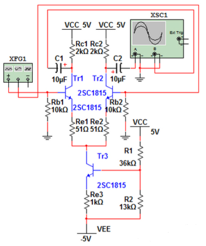
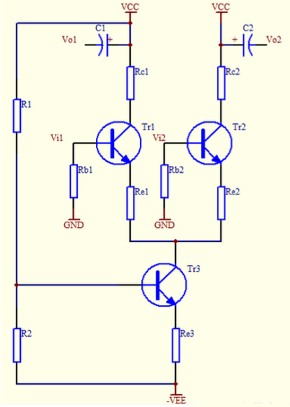
Differential Amplifier Schematic

1. The sum of Tr1 and Tr2 emitter current is a fixed value

As shown in the figure, assuming that Tr1 and Tr2 are exactly the same when there is no input signal, the respective emitter currents Ie1 and Ie2 are the same, and both are half of the emitter current of the constant current source Tr3. When a voltage is applied to input 1, Ie1 increases by ΔIe. Because Ie1+Ie2 is controlled by the constant current source Tr3, Ie2 decreases by ΔIe, that is, Ie1 and Ie2 have the same amount of change, but the direction of increase and decrease is different.


2. Amplify the difference of the input signal

The output of this circuit is taken out by the change in collector current (=emitter current) and the voltage drop on the collector resistance.

ΔIe is determined by the difference between the Vbe of Tr1 and Tr2. When the two input signals are the same, the Vbe of Tr1 and Tr2 is the same, and the difference between the two is zero, so there is no output.

When the two input signals are different, the changes of Ie1 and Ie2 are equal in magnitude and opposite in direction, so Vo1 and Vo2 are signaling with the same amplitude and opposite phase.

Therefore, the differential amplifier circuit only amplifies the difference between the two input signals and does not amplify the same input signal, so it can play a role in suppressing temperature drift.


3. The gain of the differential amplifier

The input of the differential amplifier has two forms of single-ended input and double-ended input, and the output also has two forms of single-ended output and double-ended output.

The gain of the double-ended output is: AV=RC/RE

The gain of single-ended output is: AV=RC/2RE

That is, the single-ended output gain is half of the double-ended output.

It can be seen that the gain of the differential amplifier is the same as that of the single-tube common emission amplifier. The addition of a tube does not increase the gain, but the temperature drift is well restrained.

 

2SC1815 Simulation Circuit

Simulation Circuit


The differential input voltage Vid≤100mV, the amplifier circuit gain≥20dB, that is 10 times, because the actual gain is always smaller than the theoretical calculation value, so the theoretical calculation gain is positioned at 20 times, and the maximum output voltage is 100mV×20=2V.


The power supply voltage of the differential amplifier is larger than the maximum output voltage plus the voltage drop on the emitter resistor Re3 of Tr3 working as a constant current source.


If the voltage drop of Re3 is 2V, the power supply voltage should be above 4V. In order to make the base voltage of Tr1 and Tr2 0V, remove the coupling capacitance on the input side and simplify the circuit, so a ±5V dual power supply is used.


The collector current of Tr1 and Tr2 is generally 0.1 to several milliamperes. Here is set to 1mA, then the emitter current of the constant current source Tr3 is set to 2mA. Let the voltage drop on Re3 be 2V and the current flows through 2mA, so

Re3=2V/2mA=1kΩ


In order to make the voltage drop on Re3 2V, set Vbe to 0.6V, then the voltage drop on R2 is 2.6V, so the voltage drop on R1 is 7.4V.


In order to make the base current on Tr3 negligible, the current flowing on R1 and R2 must be more than 10 times larger than the base current. If β=100, the base current of Tr3 is

Ib3=2mA/100=0.02mA


So the current flowing through R1 and R2 is 0.2mA. R1=7.4V/0.2mA=36kΩ R2=2.6V/0.2mA=13kOΩ

2SC1815 Applications

▲Use in general-purpose switching

▲Use in class B amplifiers

▲Use in pre-amplifier circuits

▲Use in push-Pull configuration circuits


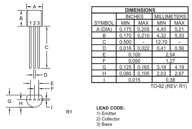
2SC1815 Mechanical Data

2SC1815 Manufacturer

Central Semiconductor is a leading provider of superior discrete semiconductors that have been applied in electronic products all over the world since 1974. Nowadays, the company's products lines contain MOSFETs, bridge rectifiers, silicon carbide devices, protection devices, rectifiers, current limiting diodes, bipolar power transistors, standard, and custom small-signal transistors, and thyristors. 


Except for the industry-standard surface mount, the company's products also support bare die, MDMs (Multi Discrete Modules™), through-hole packages. With the loyal and high-quality brand image it has built, Central keeps leveraging its service capability and benefit more and more customers through exclusive high-tech products.


Datasheet PDF

Download datasheets and manufacturer documentation for Central Semiconductor 2SC1815.

2SC1815 Documents

Download datasheets and manufacturer documentation for 2SC1815

Frequently Asked Questions

1.What triode can replace 2SC1815?
2SC1815 is one of the most commonly used NPN transistors. You can replace it with commonly used transistors such as 2N5551, 9014, and 2N3904.
2.What circuit can LM358 and triode 2SC1815 form?
LM358 is a dual operational amplifier, which integrates two amplifiers independently. Commonly, LM358 can be used in operational amplifier circuits; it can also be used as a voltage comparator. If LM358 is used as an operational amplifier, then 1815 will work in an amplifying state and play an amplifying role. If LM358 is connected as a voltage comparator, then 1815 is here as a switch.
3.The magnification and breakdown voltage of the transistor 2SC1815 is?
2SC1815 usually has two gears Y and GR. Y file magnification is 120-240, GR file magnification is 200-400 breakdown voltage is 60V.
FAQ
1.What triode can replace 2SC1815?
2SC1815 is one of the most commonly used NPN transistors. You can replace it with commonly used transistors such as 2N5551, 9014, and 2N3904.
2.What circuit can LM358 and triode 2SC1815 form?
LM358 is a dual operational amplifier, which integrates two amplifiers independently. Commonly, LM358 can be used in operational amplifier circuits; it can also be used as a voltage comparator. If LM358 is used as an operational amplifier, then 1815 will work in an amplifying state and play an amplifying role. If LM358 is connected as a voltage comparator, then 1815 is here as a switch.
3.The magnification and breakdown voltage of the transistor 2SC1815 is?
2SC1815 usually has two gears Y and GR. Y file magnification is 120-240, GR file magnification is 200-400 breakdown voltage is 60V.

TAGS

Share