ATTENTION: Due to increased demand and order volume, processing time may take an additional 1-3 business days.
HomeCommunitySubject5SGXMA3K2F40I3N Integrated Circuit: Features, Specification, Datasheet

5SGXMA3K2F40I3N Integrated Circuit: Features, Specification, Datasheet

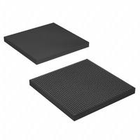
FPGA - Field Programmable Gate Array FPGA - Stratix V GX 957 LABs 696 IOs The 5SGXMA3K2F40I3N is of the Stratix V GX systems.

117

May 16, 2021

Cynthia

FPGA - Field Programmable Gate Array FPGA - Stratix V GX 957 LABs 696 IOs

The 5SGXMA3K2F40I3N is of the Stratix V GX systems. They have up to 66 integrated transceivers with a data rate of 14.1 Gbps. Backplane and optical interface implementations are also supported by these transceivers. These systems are designed for high-performance, high-bandwidth applications in the wireline, military communications, and network test equipment industries, such as 40G/100G optical transport, packet processing, and traffic management.

5SGXMA3K2F40I3N

654In Stock
Min.: 1 Mult.: 1
Price not displayed? Not available to buy online? Please send an RFQ, and we will respond immediately.
Quick Links

5SGXMA3K2F40I3N Description

An improved core architecture, optimized transceivers up to 28.05 gigabits per second (Gbps), and a specific collection of integrated hard intellectual property (IP) blocks are among the features of Altera's 28-nm Stratix® V FPGAs. Stratix V FPGAs introduce a new class of application-targeted devices that are designed for: 

• Bandwidth-intensive applications and protocols, such as PCI Express® (PCIe®) Gen3

• 40G/100G and beyond data-intensive applications 

• High-performance, high-precision digital signal processing (DSP) applications

Each of the four Stratix V variants (GT, GX, GS, and E) is aimed at a particular group of applications.

5SGXMA3K2F40I3N Features

Feature Description
Technology

• 28-nm TSMC process technology

• 0.85-V or 0.9-V core voltage

Low-power serial transceivers

• 28.05-Gbps transceivers on Stratix V GT devices

• Electronic dispersion compensation (EDC) for XFP, SFP+, QSFP, CFP optical module support 

• Adaptive linear and decision feedback equalization 

• Transmitter pre-emphasis and de-emphasis 

• Dynamic reconfiguration of individual channels 

• On-chip instrumentation (EyeQ non-intrusive data eye monitoring)

Backplane capability • 600-Megabits per second (Mbps) to 12.5-Gbps data rate capability
General-purpose I/Os (GPIOs)

• 1.6-Gbps LVDS

 • 1,066-MHz external memory interface 

• On-chip termination (OCT) 

• 1.2-V to 3.3-V interfacing for all Stratix V devices

Embedded HardCopy Block • PCIe Gen3, Gen2, and Gen1 complete protocol stack, x1/x2/x4/x8 end point and root port
Embedded transceiver hard IP

• Interlaken physical coding sublayer (PCS)

 • Gigabit Ethernet (GbE) and XAUI PCS 

• 10G Ethernet PCS • Serial RapidIO® (SRIO) PCS 

• Common Public Radio Interface (CPRI) PCS 

• Gigabit Passive Optical Networking (GPON) PCS

Power management

• Programmable Power Technology

• Quartus II integrated PowerPlay Power Analysis

High-performance core fabric

• Enhanced ALM with four registers

 • Improved routing architecture reduces congestion and improves compile times

Embedded memory blocks

• M20K: 20-Kbit with hard error correction code (ECC)

• MLAB: 640-bit

Variable precision DSP blocks

• Up to 600 MHz performance

• Natively support signal processing with precision ranging from 9x9 up to 54x54 

• New native 27x27 multiply mode 

• 64-bit accumulator and cascade for systolic finite impulse responses (FIRs) 

• Embedded internal coefficient memory 

• Pre-adder/subtractor improves efficiency 

• Increased number of outputs allows more independent multipliers

Fractional PLLs

• Fractional mode with third-order delta-sigma modulation 

• Integer mode

• Precision clock synthesis, clock delay compensation, and zero delay buffer (ZDB)

Clock networks

• 800-MHz fabric clocking

• Global, quadrant, and peripheral clock networks 

• Unused clock networks can be powered down to reduce dynamic power

Device configuration

• Serial and parallel flash interface

• Enhanced advanced encryption standard (AES) design security features 

• Tamper protection 

• Partial and dynamic reconfiguration 

• Configuration via Protocol (CvP)

High-performance packaging

• Multiple device densities with identical package footprints enables seamless migration between different FPGA densities

• FBGA packaging with on-package decoupling capacitors 

• Lead and RoHS-compliant lead-free options

HardCopy V migration

Specifications

Altera 5SGXMA3K2F40I3N technical specifications, attributes, parameters and parts with similar specifications to Altera 5SGXMA3K2F40I3N.

5SGXMA3K2F40I3N Tech Specifications

Intel 5SGXMA3K2F40I3N technical specifications, attributes, parameters and parts with similar specifications to Intel 5SGXMA3K2F40I3N.

Product Attribute Attribute Value
Factory Lead Time8 Weeks
Mounting TypeSurface Mount
Package / Case1517-BBGA, FCBGA
Surface MountYES
Number of I/Os696I/Os
Operating Temperature-40°C~100°C TJ
PackagingTray
SeriesStratix® V GX
Part StatusActive
Moisture Sensitivity Level (MSL)3 (168 Hours)
ECCN Code3A001.A.7.A
Product Attribute Attribute Value
HTS Code8542.39.00.01
Voltage - Supply0.82V~0.88V
Terminal PositionBOTTOM
Terminal FormBALL
Supply Voltage0.85V
Terminal Pitch1mm
Base Part Number5SGXMA3
JESD-30 CodeS-PBGA-B1517
Number of Outputs696Outputs
Qualification StatusNot Qualified
Power Supplies0.851.52.52.5/31.2/3V
Product Attribute Attribute Value
Number of Inputs696Inputs
Organization12830 CLBS
Programmable Logic TypeFIELD PROGRAMMABLE GATE ARRAY
Number of Logic Elements/Cells340000Logic Elements/Cells
Total RAM Bits19456000
Number of LABs/CLBs128300LABs/CLBs
Length40mm
Height Seated (Max)3.5mm
Width40mm
RoHS StatusRoHS Compliant
0 Products View Similar

5SGXMA3K2F40I3N Manufacturer

With up to 1.1 million logic components, integrated transceivers up to 28 Gbit/s, up to 1.6 Tbit/s of serial switching capacity, up to 1,840 GMACs of signal-processing performance, and up to 7 x72 DDR3 memory interfaces at 800 MHz, the Stratix series FPGAs were the company's largest and highest bandwidth devices. Northwest Logic was acquired by the company in September 2000 in order to extend its design services for the delivery of full system-on-chip solutions. Altera released the SDK for OpenCL in May 2013, allowing software developers to access the high-performance capabilities of programmable logic devices.


Datasheet PDF

Download datasheets and manufacturer documentation for Altera 5SGXMA3K2F40I3N.

5SGXMA3K2F40I3N Documents

Download datasheets and manufacturer documentation for 5SGXMA3K2F40I3N

TAGS

Share