ATTENTION: Due to increased demand and order volume, processing time may take an additional 1-3 business days.
HomeCommunitySubject74HC02 Quad 2-Input NOR Gate: 74HC02, Datasheet, Pinout

74HC02 Quad 2-Input NOR Gate: 74HC02, Datasheet, Pinout

Logic - Gates and Inverters 14-VFQFN Exposed Pad 2V~6V -40°C~125°C 74HC 5V 74HC02 0.5mm 74HC Series 6 V High Speed Si-Gate CMOS Quad 2-Input NOR Gate - DHVQFN-14

151

Nov 8, 2021

Tess Morley

7402 quad 2 input NOR gate integrated circuit 74HC02 quick look at electronics component


Logic - Gates and Inverters 14-VFQFN Exposed Pad 2V~6V -40°C~125°C 74HC 5V 74HC02 0.5mm 74HC Series 6 V High Speed Si-Gate CMOS Quad 2-Input NOR Gate - DHVQFN-14

The 74HC02 is a quad 2-input NOR gate. This article will unlock more details about 74HC02. There is a huge range of Semiconductors, Capacitors, Resistors and ICs in stock. Welcome RFQ!

74HC02BQ,115

30000In Stock
Min.: 1 Mult.: 1
Quantity Unit Price Ext. Price
1+ $0.24972$0.25
10+ $0.23559$2.36
100+ $0.22225$22.23
500+ $0.20967$104.84
1000+ $0.19781$197.81
Unit Price:$0.24972
Subtotal: $0.25
Looking for a better price? Want a lower wholesale price? Please send an RFQ, and we will respond immediately.
Quick Links

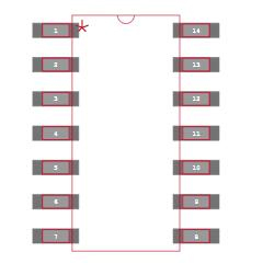
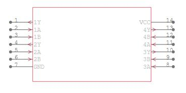
74HC02 Pinout

74HC02 CAD Model

74HC02 Symbol


74HC02 Footprint


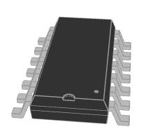
74HC02 3D Model

74HC02 Description

The 74HC02 is a quad 2-input NOR gate. Inputs include clamp diodes. This enables the use of current limiting resistors to interface inputs to voltages in excess of VCC.

74HC02 Feature

• Wide supply voltage range from 2.0 V to 6.0 V 

• CMOS low power dissipation 

• High noise immunity 

• Latch-up performance exceeds 100 mA per JESD 78 Class II Level B 

• Input levels: 

  •  For 74HC02: CMOS level 

  •  For 74HCT02: TTL level 

• Complies with JEDEC standards: 

  • JESD8C (2.7 V to 3.6 V) 

  • JESD7A (2.0 V to 6.0 V) 

• ESD protection: 

  • HBM JESD22-A114F exceeds 2000 V 

  • MM JESD22-A115-A exceeds 200 V 

• Multiple package options 

• Specified from -40 °C to +85 °C and from -40 °C to +125 °C

Specifications

Nexperia USA Inc. 74HC02BQ,115 technical specifications, attributes, parameters and parts with similar specifications to Nexperia USA Inc. 74HC02BQ,115.

74HC02BQ,115 Tech Specifications

Nexperia USA Inc. 74HC02BQ,115 technical specifications, attributes, parameters and parts with similar specifications to Nexperia USA Inc. 74HC02BQ,115.

Product Attribute Attribute Value
Factory Lead Time8 Weeks
Contact PlatingGold
MountSurface Mount
Mounting TypeSurface Mount
Package / Case14-VFQFN Exposed Pad
Number of Pins14Pins
Logic Level-High1.5V ~ 4.2V
Logic Level-Low0.5V ~ 1.8V
Operating Temperature-40°C~125°C
PackagingTape & Reel (TR)
Series74HC
Published2013
JESD-609 Codee4
Part StatusActive
Moisture Sensitivity Level (MSL)1 (Unlimited)
Product Attribute Attribute Value
Number of Terminations14Terminations
Max Power Dissipation500mW
Voltage - Supply2V~6V
Terminal PositionDUAL
Number of Functions4Functions
Supply Voltage5V
Terminal Pitch0.5mm
Base Part Number74HC02
Pin Count14
Number of Outputs1Output
Output Voltage6V
Operating Supply Voltage5V
Supply Voltage-Max (Vsup)6V
Supply Voltage-Min (Vsup)2V
Power Dissipation500mW
Product Attribute Attribute Value
Output Current25mA
Propagation Delay15 ns
Quiescent Current2μA
Turn On Delay Time7 ns
FamilyHC/UH
Logic FunctionNOR
Number of Inputs2Inputs
Logic TypeNOR Gate
Number of Gates4Gates
Max Propagation Delay @ V, Max CL15ns @ 6V, 50pF
Number of Input Lines8Input Lines
Length3mm
Radiation HardeningNo
RoHS StatusROHS3 Compliant
Lead FreeLead Free
0 Products View Similar

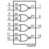
74HC02 Functional Diagram

74HC02 Functional Diagram

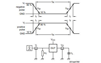
74HC02 Test Circuit

74HC02 Test Circuit

74HC02 Waveforms

Datasheet PDF

74HC02BQ,115 Documents

Download datasheets and manufacturer documentation for 74HC02BQ,115

Frequently Asked Questions

What is a 74hc02 gate?
The 74HC02; 74HCT02 is a quad 2-input NOR gate. Inputs include clamp diodes. This enables the use of current limiting resistors to interface inputs to voltages in excess of VCC.
Who owns the copyright of 74hc02 datasheet?
Note: The Copyright of this 74HC02 Datasheet belongs to Fairchild Semiconductor and is provided for information only.
When did the sn54hc02 scls076g come out?
SN74HC02, SN54HC02 SCLS076G – DECEMBER 1982 – REVISED DECEMBER 2020 An IMPORTANT NOTICE at the end of this data sheet addresses availability, warranty, changes, use in safety-critical applications, intellectual property matters and other important disclaimers.
What is NAND logic gate?
In digital electronics, a NAND gate (NOT-AND) is a logic gate that produces an output that is false only if all its inputs are true; thus its output is complemented to that of an AND gate. A LOW (0) output results only if all the inputs to the gate are HIGH (1); if any input is LOW (0), a HIGH (1) output results.
What is NAND operation?
The NAND operation is the basic logical operation performed by the solid-state transistors ("NAND gates") that underlie virtually all integrated circuits and modern computers. The first axiom system based on NAND was given by Henry Sheffer in 1913.
What is the input and output voltage range of 74HC02 OR gate chip?
The 74HC series devices have a wide operating voltage range, which can work under a voltage of 2~6V. The range of input and output levels is different for different operating voltages.
FAQ
What is a 74hc02 gate?
The 74HC02; 74HCT02 is a quad 2-input NOR gate. Inputs include clamp diodes. This enables the use of current limiting resistors to interface inputs to voltages in excess of VCC.
Who owns the copyright of 74hc02 datasheet?
Note: The Copyright of this 74HC02 Datasheet belongs to Fairchild Semiconductor and is provided for information only.
When did the sn54hc02 scls076g come out?
SN74HC02, SN54HC02 SCLS076G – DECEMBER 1982 – REVISED DECEMBER 2020 An IMPORTANT NOTICE at the end of this data sheet addresses availability, warranty, changes, use in safety-critical applications, intellectual property matters and other important disclaimers.
What is NAND logic gate?
In digital electronics, a NAND gate (NOT-AND) is a logic gate that produces an output that is false only if all its inputs are true; thus its output is complemented to that of an AND gate. A LOW (0) output results only if all the inputs to the gate are HIGH (1); if any input is LOW (0), a HIGH (1) output results.
What is NAND operation?
The NAND operation is the basic logical operation performed by the solid-state transistors ("NAND gates") that underlie virtually all integrated circuits and modern computers. The first axiom system based on NAND was given by Henry Sheffer in 1913.
What is the input and output voltage range of 74HC02 OR gate chip?
The 74HC series devices have a wide operating voltage range, which can work under a voltage of 2~6V. The range of input and output levels is different for different operating voltages.

TAGS

Share