ATTENTION: Due to increased demand and order volume, processing time may take an additional 1-3 business days.
HomeCommunitySubject74HC132 Trigger: Circuit, Pinout, and Datasheet

74HC132 Trigger: Circuit, Pinout, and Datasheet

Logic - Gates and Inverters 14-SOIC (0.154, 3.90mm Width) 2V~6V -40°C~85°C 74HC 5V Schmitt Trigger IC GATE NAND SCHMITT 4CH 14SOIC

844

Nov 11, 2021

Carol Penn

7410 74HC10 Triple 3 input NAND gate integrated circuit IC demonstration by electronzap electronics


Logic - Gates and Inverters 14-SOIC (0.154, 3.90mm Width) 2V~6V -40°C~85°C 74HC 5V Schmitt Trigger IC GATE NAND SCHMITT 4CH 14SOIC

The 74HC132 is a silicon gate C²MOS-fabricated high-speed CMOS 2-INPUT NAND SCHMITT TRIGGER GATE. This article mainly introduces circuit, pinout, datasheet and other detailed information about Toshiba Semiconductor and Storage 74HC132.
74HC132D

21000In Stock
Min.: 1 Mult.: 1
Quantity Unit Price Ext. Price
1+ $0.40676$0.41
10+ $0.38374$3.84
100+ $0.36202$36.2
500+ $0.34152$170.76
1000+ $0.32219$322.19
Unit Price:$0.40676
Subtotal: $0.41
Looking for a better price? Want a lower wholesale price? Please send an RFQ, and we will respond immediately.
Quick Links

74HC132 Description

The 74HC132 is a silicon gate C²MOS-fabricated high-speed CMOS 2-INPUT NAND SCHMITT TRIGGER GATE. It achieves high-speed operation comparable to LSTTL while keeping CMOS low power dissipation.

The 74HC132 has the same pin arrangement and function as the 74HC00D, but the inputs have a 25% VCC hysteresis and may be used as a line receiver for sluggish input signals thanks to its schmitt trigger inputs.

Static discharge and transient excess voltage safety circuits are installed on all inputs.

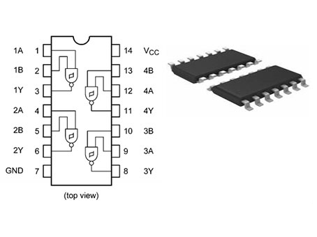
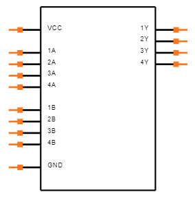
74HC132 Pinout

Pin Number Pin Name Description
1 1A Channel 1, Input A
2 1B Channel 1, Input B
3 1Y Channel 1, Output Y
4 2A Channel 2, Input A
5 2B Channel 2, Input B
6 2Y Channel 2, Output Y
7 GND Ground
8 3Y Channel 3, Output Y
9 3A Channel 3, Input A
10 3B Channel 3, Input B
11 4Y Channel 4, Output Y
12 4A Channel 4, Input A
13 4B Channel 4, Input B
14 VCC Positive Supply

74HC132 CAD Model

Symbol

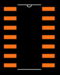
Footprint

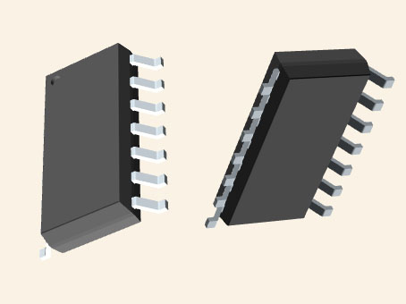
3D Model

74HC132 Features

• High speed: tpd = 11 ns (typ.) at VCC = 5 V

• Low power dissipation: ICC = 1.0 µA (max) at Ta = 25°C

• High noise immunity: VH = 1.1 V (typ.) at VCC = 4.5 V

• Balanced propagation delays: tPLH ≈ tPHL

• Wide operating voltage range: VCC(opr) = 2.0 to 6.0 V

• Unlimited input rise and fall times

• Latch-up performance exceeds 100 mA per JESD 78 Class II Level B

• Complies with JEDEC standards:

- JESD8C (2.7 V to 3.6 V)

- JESD7A (2.0 V to 6.0 V)

• ESD protection:

- HBM JESD22-A114F exceeds 2000 V

- MM JESD22-A115-A exceeds 200 V

• Multiple package options

• Specified from −40 °C to +85 °C and from −40 °C to +125 °C

Specifications

Toshiba Semiconductor and Storage 74HC132D technical specifications, attributes, parameters and parts with similar specifications to Toshiba Semiconductor and Storage 74HC132D.

74HC132D Tech Specifications

Toshiba Semiconductor and Storage 74HC132D technical specifications, attributes, parameters and parts with similar specifications to Toshiba Semiconductor and Storage 74HC132D.

Product Attribute Attribute Value
Factory Lead Time12 Weeks
Mounting TypeSurface Mount
Package / Case14-SOIC (0.154, 3.90mm Width)
Surface MountYES
Usage LevelIndustrial grade
Operating Temperature-40°C~85°C
PackagingCut Tape (CT)
Series74HC
Published2016
Part StatusActive
Moisture Sensitivity Level (MSL)1 (Unlimited)
Product Attribute Attribute Value
Number of Terminations14Terminations
Voltage - Supply2V~6V
Terminal PositionDUAL
Terminal FormGULL WING
Peak Reflow Temperature (Cel)NOT SPECIFIED
Number of Functions4Functions
Supply Voltage5V
Time@Peak Reflow Temperature-Max (s)NOT SPECIFIED
Supply Voltage-Max (Vsup)6V
Supply Voltage-Min (Vsup)2V
Number of Circuits4Circuits
Product Attribute Attribute Value
FamilyHC/UH
Number of Inputs2Inputs
Logic TypeNAND Gate
Max Propagation Delay @ V, Max CL19ns @ 5V, 50pF
Current - Quiescent (Max)1μA
FeaturesSchmitt Trigger
Length8.65mm
Height Seated (Max)1.75mm
Width3.9mm
RoHS StatusRoHS Compliant
0 Products View Similar

74HC132 Voltage Doubler Circuit

Using the electronic design below, you may construct a voltage doubler circuit. This electrical circuit, which uses the 74HC132 or 74HCT132 circuit type, has a very cheap manufacturing cost. Only four components, C4, C5, D1, and D2, are required to produce a voltage of 10 V to 5 V when the CLK signal is sent through the buffer. Two additional components, R1 and C3, are necessary if the power oscillator is to be created from an unused gate.

The table below lists the most crucial circuit parameters.

Circuit Diagram


74HC132 Alternatives

Part Number Description Manufacturer
74HC132PWLOGIC NAND Gate, HC/UH Series, 4-Func, 2-Input, CMOS, PDSO14 Nexperia
74HC132PW-TLOGIC IC HC/UH SERIES, QUAD 2-INPUT NAND GATE, PDSO14, SOT-402-1, TSSOP-14, Gate NXP Semiconductors
MC74HC132ADTR2GLOGIC Quad 2-Input NAND Gate with Schmitt Trigger Input, TSSOP-14, 2500-REEL onsemi

74HC132 Applications

• Wave and Pulse Shapers

• Astable Multivibrators

• Monostable Multivibrators

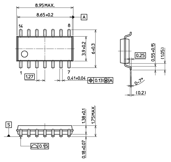
74HC132 Package

74HC132 Manufacturer

Toshiba Semiconductor & Storage provides a wide range of supporting technology solutions that enable OEMs, ODMs, CMs, and fabless semiconductor businesses to create innovative integrated products for industries such as computers, networking, communications, digital consumer, automotive, and others.

Frequently Asked Questions

1.What chip is 74HC132?
74HC132 is a quad 2 input terminal and non-Schmitt trigger, CMOS device, power supply operating voltage 2V ~ 6V.
2.If the motherboard power-on circuit is broken, what type of replacement should be used for 74HC132?
74HC132 is a four 2-input NAND gate (Schmidt input). Which model can be used instead depends on the specific circuit. For example, if all the logic devices in the original circuit are TTL circuits, 74HCT132D can also be used. If the operating voltage of the original circuit is in the range of 2V~5.5V, 74AHC132D can also be used. There are also many Schmidt input NAND gates with slight differences in operating voltage and speed. The pins are compatible with 74HC132, such as 74VHC132, 74AC132, 74LVX132, etc. Even 74HC00 is not absolutely irreplaceable. 74HC132 is also pin-compatible, the only difference is that it is not Schmidt input. So everything depends on the specific conditions of the actual circuit.
3.What is the role of 74HC132?
74HC132 is four 2-input terminals with non-Schmitt triggers. The function is the NAND operation of 2 inputs, which must meet the NAND operation under the input and output conditions of the Schmitt trigger.
FAQ
1.What chip is 74HC132?
74HC132 is a quad 2 input terminal and non-Schmitt trigger, CMOS device, power supply operating voltage 2V ~ 6V.
2.If the motherboard power-on circuit is broken, what type of replacement should be used for 74HC132?
74HC132 is a four 2-input NAND gate (Schmidt input). Which model can be used instead depends on the specific circuit. For example, if all the logic devices in the original circuit are TTL circuits, 74HCT132D can also be used. If the operating voltage of the original circuit is in the range of 2V~5.5V, 74AHC132D can also be used. There are also many Schmidt input NAND gates with slight differences in operating voltage and speed. The pins are compatible with 74HC132, such as 74VHC132, 74AC132, 74LVX132, etc. Even 74HC00 is not absolutely irreplaceable. 74HC132 is also pin-compatible, the only difference is that it is not Schmidt input. So everything depends on the specific conditions of the actual circuit.
3.What is the role of 74HC132?
74HC132 is four 2-input terminals with non-Schmitt triggers. The function is the NAND operation of 2 inputs, which must meet the NAND operation under the input and output conditions of the Schmitt trigger.

TAGS

Share