ATTENTION: Due to increased demand and order volume, processing time may take an additional 1-3 business days.
HomeCommunitySubject74HC595 Shift Register IC : Pinout, Advantage and Datasheet

74HC595 Shift Register IC : Pinout, Advantage and Datasheet

IC SHIFT REGISTER 8BIT 16SOIC Hi, fellas. Welcome back to the post about electronic components today. 74HC595 IC is a 16-pin shift register IC based on CMOS.

123

Sep 6, 2021

James Locke

74HC595 & 74HC165 Shift Registers with Arduino


IC SHIFT REGISTER 8BIT 16SOIC

Hi, fellas. Welcome back to the post about electronic components today. 74HC595 IC is a 16-pin shift register IC based on CMOS. It is consisting of a D-type latch along with a shift register inside the chip. This article mainly introduces pinout, advantage, datasheet and other detailed information about Nexperia USA 74HC595.

74HC595D,118

1300000In Stock
Min.: 1 Mult.: 1
Quantity Unit Price Ext. Price
1+ $0.26536$0.27
10+ $0.25034$2.5
100+ $0.23617$23.62
500+ $0.2228$111.4
1000+ $0.21019$210.19
Unit Price:$0.26536
Subtotal: $0.27
Looking for a better price? Want a lower wholesale price? Please send an RFQ, and we will respond immediately.
Quick Links

74HC595 Description

74HC595 IC is a 16-pin shift register IC based on CMOS. It is consisting of a D-type latch along with a shift register inside the chip. It receives serial input data and then sends out this data through parallel pins. 


In addition to parallel outputs, it also provides a serial output. It has independent clock inputs for the shift register and D latch. This IC belongs to the HC family of logic devices which is designed for use in CMOS applications. 


74HC595 has two built-in registers. The first one is a shift register and the second one is a storage register. Data serially transfers to shift register bit by bit. But it transfers to the storage register only when the data latch pin is active high.


74HC595 has a very wide range of applications in daily life. It can be used as a serial to parallel data converter, can receive and keeps the data for a long time, etc. Moreover, It can be used in home appliances, for industrial management, as computer peripheral.

74HC595 Pinout


Pin Number Pin Name Description
15, 1, 2, 3, 4, 5, 6, 7 Q0, Q1, Q2, Q3, Q4, Q5, Q6, Q7 parallel data output
8 GND ground (0 V)
9 Q7S serial data output
10 MR master reset (active LOW)
11 SHCP shift register clock input
12 STCP storage register clock input
13 OE output enable input (active LOW)
14 DS serial data input
15 Q0 parallel data output 0
16 VCC supply voltage

74HC595 Pin Description

74HC595 CAD Model

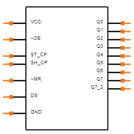
Symbol

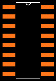
Footprint

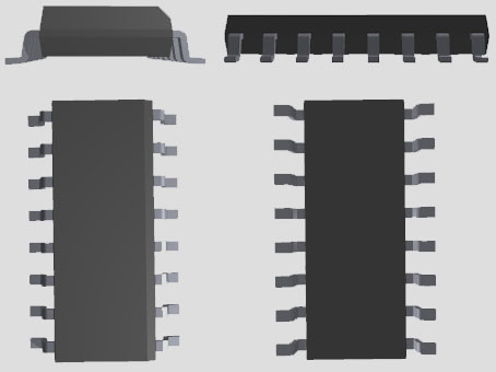
3D Model

74HC595 Features

●Operating voltage ranges from 2V – 6V

●Clock frequency max is 25 MHz at 4.5V

●Power utilization is 80uA

●To get more outputs, we can simply cascade through more chips

●The sink current is 35mA

●Low-level input voltage Max: 1.35V

●High-level i/p voltage min 3.15V

●Max quiescent current is 80 µA

●Max input current is 1µA

●Shift frequency is DC-30 MHz

●The output voltage is equal to the operating voltage

●High noise immunity.

●Available in different packages like 16-pin GDIP, PDIP & PDSO

Specifications

Nexperia USA Inc. 74HC595D,118 technical specifications, attributes, parameters and parts with similar specifications to Nexperia USA Inc. 74HC595D,118.

74HC595D,118 Tech Specifications

Nexperia USA Inc. 74HC595D,118 technical specifications, attributes, parameters and parts with similar specifications to Nexperia USA Inc. 74HC595D,118.

Product Attribute Attribute Value
Factory Lead Time4 Weeks
Mounting TypeSurface Mount
Package / Case16-SOIC (0.154, 3.90mm Width)
Surface MountYES
Number of Pins16Pins
Number of Elements1 Element
Operating Temperature-40°C~125°C
PackagingTape & Reel (TR)
Series74HC
JESD-609 Codee4
Part StatusActive
Moisture Sensitivity Level (MSL)1 (Unlimited)
Number of Terminations16Terminations
Product Attribute Attribute Value
Terminal FinishNickel/Palladium/Gold (Ni/Pd/Au)
Additional FeatureSERIAL STANDARD OUTPUT FOR CASCADING
Voltage - Supply2V~6V
Terminal PositionDUAL
Terminal FormGULL WING
Supply Voltage5V
Frequency100MHz
Base Part Number74HC595
FunctionSerial to Parallel, Serial
Output TypeTri-State
Supply Voltage-Max (Vsup)6V
Supply Voltage-Min (Vsup)2V
FamilyHC/UH
Product Attribute Attribute Value
Logic FunctionShift Register
Output Characteristics3-STATE
Logic TypeShift Register
Output PolarityTRUE
Number of Bits per Element8Bits per Elements
Trigger TypePOSITIVE EDGE
Propagation Delay (tpd)265 ns
fmax-Min24 MHz
Count DirectionRIGHT
Length9.9mm
Width3.9mm
RoHS StatusROHS3 Compliant
0 Products View Similar

74HC595 Alternatives

Part Number Description Manufacturer
935009160112LOGIC IC HC/UH SERIES, 8-BIT RIGHT SERIAL IN PARALLEL OUT SHIFT REGISTER, TRUE OUTPUT, PDSO16, 3.90 MM, PLASTIC, MS-012AC, SOT-109-1, SO-16, Shift Register NXP Semiconductors
935009160118LOGIC Serial In Parallel Out, HC/UH Series, 8-Bit, Right Direction, True Output, CMOS, PDSO16 Nexperia

Where to use 74HC595?

Do you ever wonder, how an embedded engineer controls hundreds of series or parallel connected light-emitting diodes with the help of a microcontroller that have very few general-purpose I/O pins? Additionally, You want to control more than 8 servo motors and you have only 2-3 GPIO pins of a microcontroller. How you will solve this problem? How you will control an LED Matrix of different dimensions such as 8×8, 16×16, 32×32 with minimum GPIO pins of a microcontroller? The simple answer is a 74HC595 shift register.


In most of the applications, you need more outputs for interfacing LEDs or any other devices such as seven segments, 16 segments, LED flasher, etc. This IC is very handy to use. For increasing the output pins, you can interface this IC with different microcontrollers such as Arduino Uno, PIC Microcontroller, Atmel, etc. You can use this IC in designing projects which require controlling multiple outputs.

How to use 74HC595?

74HC595 has eight outputs and 3 input pins which include a data pin, storage resistor clock pin, and shift register clock pin. Connect pin8 to ground and pin16 to +5V voltage supply.


The output enables pin (~OE) should be grounded to enable the output pins of the shift register. The master reset pin will clear the memory of a shift register if it is applied with a low signal. That’s why it should be kept high.


When the positive edge transition occurs on pin 11, the shift register will accept the inputs applied on the data line.

The outputs of the storage register are connected to the input pins of the D-latch/storage resistor.


These inputs are updated on the latch output when a positive edge transition occurs at pin 12.

Most importantly, If you need to cascade multiple IC’s together then pin 9 is connected to the data pin of another shift register IC.


74HC595 Advantages

-Very quick to use

-It is employed within CDMA for generating Pseudo Noise Sequence Numbers.

-The data can be converted very easily as compared to converter circuits

-The signal delay can be done by using this shift register

-Simple to design

-This can be used to encrypt/decrypt the data.

-The data can be tracked

-The disadvantage of a shift register is, the output current strength is not strong

74HC595 Applications

-Used to drive a number of LEDs servers

-Used to Capture & Hold Logic

-Used in Network Switches

-Used in Simple Data Conversion from Serial to Parallel

-Used in Controlling in Industries

-Used in Extending the GPIO Pin on an MCU/MPU

-Used in Electronic Devices

-Used in Power Infrastructure

-Used in LED Matrix or Cube Projects

-Used in Cascading Applications

-Used in Interfacing LCD

-Used in High logic level controller

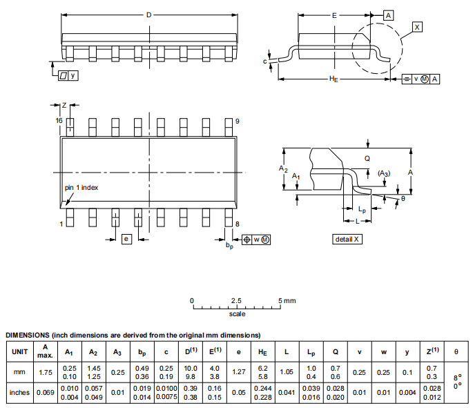
74HC595 Package

74HC595 Manufacturer

NXP Semiconductors N.V. is a Dutch semiconductor manufacturer with headquarters in Eindhoven, Netherlands that focuses on the automotive industry. The company employs approximately 31,000 people in more than 35 countries, including 11,200 engineers in 33 countries. NXP reported revenue of $9.4 billion in 2018.


Datasheet PDF

74HC595D,118 Documents

Download datasheets and manufacturer documentation for 74HC595D,118

Frequently Asked Questions

1.What is the difference between 74HC595 and 74HC138?
The difference between 74HC595 and 74HC138 is: The two are completely different things. 74HC595 is an 8-bit shift register with only one regular input terminal, the other two are the set terminal and the pulse input terminal, and have four output terminals; 74HC138 is a 3-wire-8-line decoder with three regular input terminals, others are all set input terminals, and there are eight output terminals.
2.What chip is 74HC595?
It is a 16-pin integrated circuit chip, which is an 8-bit shift register that is serial in and out.
3.Can the unused pin of 74HC595 be grounded?
Yes, no problem, but the power and ground should be connected.
FAQ
1.What is the difference between 74HC595 and 74HC138?
The difference between 74HC595 and 74HC138 is: The two are completely different things. 74HC595 is an 8-bit shift register with only one regular input terminal, the other two are the set terminal and the pulse input terminal, and have four output terminals; 74HC138 is a 3-wire-8-line decoder with three regular input terminals, others are all set input terminals, and there are eight output terminals.
2.What chip is 74HC595?
It is a 16-pin integrated circuit chip, which is an 8-bit shift register that is serial in and out.
3.Can the unused pin of 74HC595 be grounded?
Yes, no problem, but the power and ground should be connected.

TAGS

Share