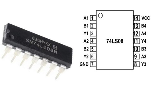
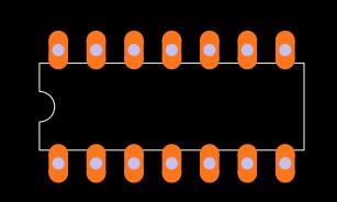
To comprehend the 74LS08 AND gate IC, we must first comprehend the operation of a single AND logic gate. In general, an AND logic gate consists of three sorts of combinations, each of which has similar outputs on specific inputs.
Below is a diagram of a transistor-based logic AND gate circuit. Two transistors are utilized as switches in the following circuit to change the output condition for different inputs. Both transistors in the IC 74LS08 AND logic gate are linked in series. The power is applied to the collector terminal of the first transistor, and the output is obtained at the emitter terminal of the second transistor.

74LS08 Input Voltage
The two inputs are connected to the base terminal of both transistors. The inputs allow the current to travel between the two transistors. When the input signal is HIGH, current flows through the transistor, resulting in full voltages on the o/p pin.
In other cases, if one of the circuit's input pins is LOW, the o/p will also be LOW due to the current supply from the transistors. The output here will not be dependent on the type of AND gate, but will always be determined by the truth table of the AND gate, which is shown below.
A single AND gate or a combination of two AND gates cannot be used to create another logic gate, however, an AND logic gate can be used to create additional logic gates.
With just one NOT gate, an AND logic gate can be changed to a NAND logic gate. Other logic gates, such as XNOR and XOR, rely on AND logic gates; nevertheless, OR and NOT logic gates are required to create other logic gates.