ATTENTION: Due to increased demand and order volume, processing time may take an additional 1-3 business days.
HomeCommunitySubject74LS164 Parallel-Out Shift Register IC: Datasheet, Schematic and Pinout

74LS164 Parallel-Out Shift Register IC: Datasheet, Schematic and Pinout

Shift Register Function:Serial to Parallel The 74LS164 is a high-speed 8-Bit Serial-In Parallel-Out Shift Register. This post mainly covers schematic, pinout, datasheet, circuit, and other details about the 74LS164 shift register. Furthermore, there is a huge range of semiconductors, capacitors, resistors, and ICs in stock. Welcome your RFQ!
297

Oct 5, 2021

Sherry Titus

FUNCIONAMIENTO DEL REGISTRO 74LS164


Shift Register Function:Serial to Parallel

The 74LS164 is a high-speed 8-Bit Serial-In Parallel-Out Shift Register. This post mainly covers schematic, pinout, datasheet, circuit, and other details about the 74LS164 shift register. Furthermore, there is a huge range of semiconductors, capacitors, resistors, and ICs in stock. Welcome your RFQ!


SN74LS164D

2300In Stock
Min.: 1 Mult.: 1
Quantity Unit Price Ext. Price
1+ $0.83174$0.83
10+ $0.78466$7.85
100+ $0.74025$74.02
500+ $0.69835$349.18
1000+ $0.65882$658.82
Unit Price:$0.83174
Subtotal: $0.83
Looking for a better price? Want a lower wholesale price? Please send an RFQ, and we will respond immediately.
Quick Links

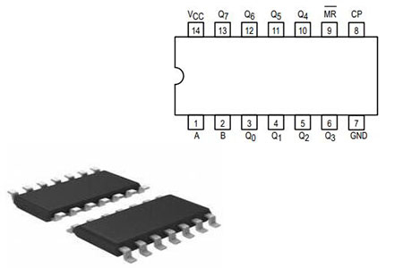
74LS164 Pinout

74LS164 Pinout


Pin No Pin Name Description
1 A Data Input Pin A
2 B Data Input Pin B
3 Q0 Output pin Q0
4 Q1 Output pin Q1
5 Q2 Output pin Q2
6 Q3 Output pin Q3
7 GND Ground Pin
8 CP Clock Pulse Input
9 MR’ Active Low Master   Reset
10 Q4 Output pin Q4
11 Q5 Output pin Q5
12 Q6 Output pin Q6
13 Q7 Output pin Q7
14 Vcc Chip Supply Voltage

What is 74LS164?

The 74LS164 is an 8-bit Serial-In Parallel-Out Shift Register with excellent speed. Serial data is inputted via a two-input AND gate that is timed to the clock's LOW to HIGH transition. The device has an asynchronous Master Reset feature that clears the register and sets all outputs to LOW regardless of the clock. It achieves high speeds by using a Schottky diode clamped method and is completely compatible with all Motorola TTL products.

74LS164 Logic Diagram

The 74LS164 shift register IC's logic diagram is represented in the diagram below. It has eight flip-flops, one AND gate, and two Not gates on the inside.


74LS164 Logic Diagram 

74LS164 Features

  • Operating Voltage: 3V to 18V

  • Supply Voltage – Max: 5.25 V

  • Propagation Delay Time: 25 ns

  • Max. Clock Frequency: 36 MHz

  • Operating Temperature Range: 0C to + 70 C

  • Fully Buffered Clock

  • Available in 16-pin PDIP, GDIP, PDSO packages

Specifications

SN74LS164D Tech Specifications

Texas Instruments SN74LS164D technical specifications, attributes, parameters and parts with similar specifications to Texas Instruments SN74LS164D.

Product Attribute Attribute Value
Lifecycle StatusACTIVE (Last Updated: 1 day ago)
Factory Lead Time6 Weeks
MountSurface Mount
Mounting TypeSurface Mount
Package / Case14-SOIC (0.154, 3.90mm Width)
Number of Pins14Pins
Weight129.387224mg
Number of Elements1 Element
Operating Temperature0°C~70°C
PackagingTube
Series74LS
JESD-609 Codee4
Pbfree Codeyes
Part StatusActive
Moisture Sensitivity Level (MSL)1 (Unlimited)
Number of Terminations14Terminations
ECCN CodeEAR99
Product Attribute Attribute Value
Terminal FinishNickel/Palladium/Gold (Ni/Pd/Au)
Additional FeatureGATED SERIAL INPUTS (A AND B)
Voltage - Supply4.75V~5.25V
Terminal PositionDUAL
Terminal FormGULL WING
Peak Reflow Temperature (Cel)260
Supply Voltage5V
Frequency36MHz
Base Part Number74LS164
FunctionSerial to Parallel
Output TypePush-Pull
Operating Supply Voltage5V
Power Supplies5V
Number of Circuits2Circuits
Propagation Delay32 ns
Turn On Delay Time36 ns
FamilyLS
Product Attribute Attribute Value
Logic FunctionShift Register
DirectionUnidirectional
Logic TypeShift Register
Output PolarityTRUE
Number of Bits per Element8Bits per Elements
Trigger TypePOSITIVE EDGE
Schmitt TriggerNo
Input Current100μA
Number of Output Lines3Output Lines
Height1.75mm
Length8.65mm
Width3.91mm
Thickness1.58mm
REACH SVHCNo SVHC
Radiation HardeningNo
RoHS StatusROHS3 Compliant
Lead FreeLead Free
0 Products View Similar

74LS164 Applications

  • Arithmetic-unit registers

  • Sequence generators

  • Control circuits

  • Digital up to and down counters

  • Shift-left — shift right registers

  • Serial-to-parallel/parallel-to-serial conversions

  • Sequence generation


Working Principle of 74LS164 Shift Register

  • ~MR is a low-input active master reset pin. The output will be in a low state until its state is low, regardless of what is at input A or B. As a result, it's also known as the Reset or Clear mode of operation. MR must be set to a high value to complete the procedure.

  • Serial data can be sent by either of the two input pins while using another pin as an active high allows data to be entered into other input pins. Any input pin that isn't in use needs to be set to high. Connecting two input pins is also conceivable.

  • When a clock transitions from low to high, Data moves one position to the right, and Q0 is filled with the AND of two data inputs at A and B.


Where to Use 74LS164

The 74LS164 Shift Register is an 8-bit serial-in, parallel-out device. It can receive (input), obtain data serially, and control output pins in parallel, which means it can receive (input), get data serially and control output pins in parallel. This is useful when our MCU/MPU does not have enough GPIO pins to control the needed number of outputs. It's frequently used in projects where a huge number of LEDs must be controlled by a microcontroller. Because it may operate as the data bit for LCDs, it can also be utilized to interface an LCD panel.


How to Use 74LS164

To extend GIPO functionality, the 74LS164 shift register is typically utilized with microcontrollers or microprocessors. The 74LS164 is a 14-pin integrated circuit with four inputs, eight outputs, power, and ground. A microcontroller with four lines is required for the 74LS164. There are three input pins: one for the clock, one for the clear, and two for the input (A & B). Input Pins A and B function as a logical AND gate, meaning it will read 1 if both pins are logic high (5 volts). To clear the full register at once, use the clear pin.

74LS164 Circuit


74LS164 Package

74LS164 Package

74LS164 Manufacturer

Texas Instruments (TI) emerges as a globally recognized semiconductor manufacturer expanded into 35 countries. It has seen rapid growth. In 1958, TIer firstly introduced the working integrated circuit. And today more than 30,000 TIers worldwide are committed to designing, manufacturing, and selling analog and embedded processing chips. They aspire to solve challenges as well as change the world through their technologies.

Frequently Asked Questions

What is the use of 74LS164?
The 74LS164 is a high-speed 8-Bit Serial-In Parallel-Out Shift Register. The input Serial data is given through a 2-Input AND gate synchronous with the LOW to HIGH transition of the clock. The IC also features gated serial inputs and an asynchronous clear pin.
How does 74LS164 work?
74LS164 is a high-speed 8-Bit Serial-In Parallel-Out Shift Register. Serial data is entered through a 2-Input AND gate synchronous with the LOW to HIGH transition of the clock. The device features an asynchronous Master Reset which clears the register setting all outputs LOW independent of the clock.
How many pins are there in 74LS164?
The SN74LS164 is a 14 pin IC; it has 4 input pins, 8 output pins, power, and ground.
What is the higher driving capability of 74LS164 and 74HC164?
74LS164 is a TTL device with a high-level driving capability of about 0.4mA and a low-level driving capability of about 8mA. 74HC164 is a CMOS device; both high-level and low-level drive capabilities can reach 20mA.
FAQ
What is the use of 74LS164?
The 74LS164 is a high-speed 8-Bit Serial-In Parallel-Out Shift Register. The input Serial data is given through a 2-Input AND gate synchronous with the LOW to HIGH transition of the clock. The IC also features gated serial inputs and an asynchronous clear pin.
How does 74LS164 work?
74LS164 is a high-speed 8-Bit Serial-In Parallel-Out Shift Register. Serial data is entered through a 2-Input AND gate synchronous with the LOW to HIGH transition of the clock. The device features an asynchronous Master Reset which clears the register setting all outputs LOW independent of the clock.
How many pins are there in 74LS164?
The SN74LS164 is a 14 pin IC; it has 4 input pins, 8 output pins, power, and ground.
What is the higher driving capability of 74LS164 and 74HC164?
74LS164 is a TTL device with a high-level driving capability of about 0.4mA and a low-level driving capability of about 8mA. 74HC164 is a CMOS device; both high-level and low-level drive capabilities can reach 20mA.

TAGS

Share