ATTENTION: Due to increased demand and order volume, processing time may take an additional 1-3 business days.
HomeCommunitySubject74LS73 Dual JK Flip-Flop IC: Datasheet, Pinout and How Do Flip Flops Work

74LS73 Dual JK Flip-Flop IC: Datasheet, Pinout and How Do Flip Flops Work

The 74LS73 is a dual J-K Flip-flop with clear with LS technology and two independent J-K flip-flops with individual J-K, clock, and direct clear inputs. This article mainly explains datasheet, pinout, application, working, and other details about 74LS73 flip-flop.

8698

Nov 1, 2021

Ula Romeo

JK Flip-flop Circuit & Working Explained

The 74LS73 is a dual J-K Flip-flop with clear with LS technology and two independent J-K flip-flops with individual J-K, clock, and direct clear inputs. This article mainly explains datasheet, pinout, application, working, and other details about 74LS73 flip-flop.

74LS73N

Inquiry
Min.: 1 Mult.: 1
Price not displayed? Not available to buy online? Please send an RFQ, and we will respond immediately.
Quick Links

What is 74LS73?

The 74LS73 is a twin J-K flip-flop with clear and LS technology, as well as two independent J-K flip-flops having J-K, clock, and direct clear inputs. Two negative-edge-triggered flip-flops are included in the LS73A. For predictable functioning, the J and K inputs must be steady one setup time before the high-to-low clock change. When the clear is low, the clock and data inputs are overridden, causing the Q output to be low and the Q output to be high.

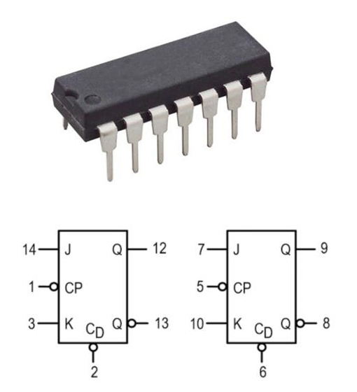
74LS73 Pin

74LS73 Pin


Pin No Pin Name Description
1 CLK1 Clock input pin 1
2 CLR1― Active low clear pin   1
3 K1 Input pin K1
4 VCC Supply Voltage
5 CLK2 Clock input pin 2
6 CLR2― Active low clear pin   2
7 J2 Input pin J2
8 Q2― Active low output 2   pin
9 Q2 Active high output 2   pin
10 K2 Input pin K2
11 GND Ground Pin
12 Q1 Active high output 1   pin
13 Q1― Active low output 1   pin
14 J1 Input pin J1

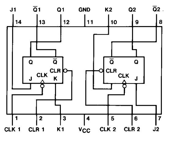
74LS73 Connection Diagram

74LS73 Connection Diagram

Specifications

74LS73N Tech Specifications

RAYTHEON SEMICONDUCTOR 74LS73N technical specifications, attributes, parameters and parts with similar specifications to RAYTHEON SEMICONDUCTOR 74LS73N.

Product Attribute Attribute Value
Surface MountNO
Number of Terminals14Terminals
Operating Temperature (Max.)70°C
JESD-609 Codee0
Terminal FinishTin/Lead (Sn/Pb)
Terminal PositionDUAL
Product Attribute Attribute Value
Terminal FormTHROUGH-HOLE
Number of Functions2Functions
Supply Voltage5V
Terminal Pitch2.54mm
JESD-30 CodeR-PDIP-T14
Qualification StatusNot Qualified
Product Attribute Attribute Value
Power Supplies5V
Temperature GradeCOMMERCIAL
Logic IC TypeJ-K FLIP-FLOP
Trigger TypeNEGATIVE EDGE
RoHS StatusNon-RoHS Compliant
0 Products View Similar

74LS73 Features

  • Dual JK Flip Flop Package IC

  • Operating Voltage: 5V

  • High-Level Input Voltage: 2 V

  • Low-Level Input Voltage: 0.8 V

  • Operating temperature range = -55 to 125°C

  • Available in 14-pin PDIP, GDIP, PDSO packages

74LS73 Applications

  • Shift Registers

  • PCs and notebooks

  • Digital Electronics

  • Network equipment

  • Memory/Control Registers

  • EEPROM circuits

  • Latching devices

Where to Use 74LS73?

The 74LS73 is a JK flip flop IC with two in-line lines. It contains two JK flip flops, each of which can be used independently depending on our purpose. When the clock is high, the J-K input is loaded into the master, and when the clock is low, it is transferred to the slave. For your project, this IC can be used in latching applications or as a small programmable memory.

How to Use 74LS73?

Here shows a typical sample connection for the working of 74LS73 JK Flip-Flops.
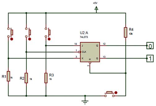
74LS73 Circuit

The J and K pins are the Flip-input Flop's pins, while the Q and Q bar pins are its output pins. Through the use of a 1k resistor, input pins are brought down to the ground, preventing the pin from floating. When the button is not pressed, the pin is held to the ground, and when the button is pressed, the pin is held to supply voltage.

The reset button should be pulled up with a 1K resistor, and when grounded, the flip-flop will be reset. The JK flip-clock flop's signal is responsible for changing the output's state. Only the rising edge of the clock signal will cause the flip-flop to change its output.

 

74LS73 Equivalents

MC74HC73A, 74LS76, 74LS107, 4027B

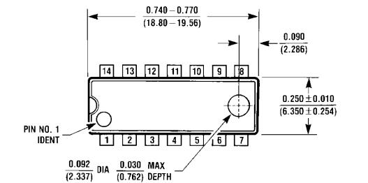
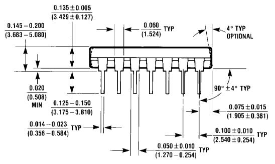
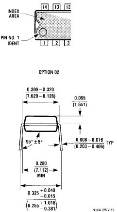
74LS73 Package Dimensions

74LS73 Package Dimensions

74LS73 Manufacturer

Raytheon's Semiconductor Division was established in Mountain View, California, in 1968 by its parent company, Raytheon Company of Lexington, Massachusetts, which is 1990, was described as"one of the largest and most diversified electronics companies in the United States." In the early 1990s, the company was involved in the manufacture and distribution of semiconductors and had 1200 employees at its Mountain View location. In November of 1997, Raytheon sold its Semi-Conductors/Integrated Circuits Division to the Fairchild Semiconductor Corporation.

Frequently Asked Questions

What is the use of 74LS73?
The 74LS73 is a dual in-line JK flip flop IC. It contains two independent negative-edge-triggered J-K flip-flops with individual J-K, clock, and direct clear inputs. The J and K inputs must be stable one setup time before the high-to-low clock transition for predictable operation.
How many pins are there in 74ls73?
It is available in 14-pin PDIP, GDIP, PDSO packages.
How does 74LS73 Flip-flop work?
The JK flip flop work as a T-type toggle flip flop when both of its inputs are set to 1. The JK flip flop is an improved clocked SR flip flop. But it still suffers from the "race" problem. This problem occurs when the state of the output Q is changed before the clock input's timing pulse has time to go "Off"
What is the voltage of 74LS73?
Its operating voltage is 5V and its high-level input voltage is 2 V.
FAQ
What is the use of 74LS73?
The 74LS73 is a dual in-line JK flip flop IC. It contains two independent negative-edge-triggered J-K flip-flops with individual J-K, clock, and direct clear inputs. The J and K inputs must be stable one setup time before the high-to-low clock transition for predictable operation.
How many pins are there in 74ls73?
It is available in 14-pin PDIP, GDIP, PDSO packages.
How does 74LS73 Flip-flop work?
The JK flip flop work as a T-type toggle flip flop when both of its inputs are set to 1. The JK flip flop is an improved clocked SR flip flop. But it still suffers from the "race" problem. This problem occurs when the state of the output Q is changed before the clock input's timing pulse has time to go "Off"
What is the voltage of 74LS73?
Its operating voltage is 5V and its high-level input voltage is 2 V.

TAGS

Share