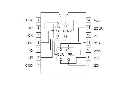
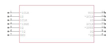
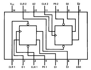
It is rather simple to use a Flip-Flop. Simply use the Vcc and GND pins to power the IC. As previously stated, each flip-flop works separately; simply connect the input signals 2 and 3 to use the first flip-flop, and the output will be at pins 5 and 6. A clock source should be given for pin 3, which is usually a PWM signal from an MCU or 555 timers. By making the pin high, you can clear the data and reset the flip flop. Taking a look at the function table below will help you understand how the Flip flop works. The symbol "X" stands for "don't care," while the up-arrow represents the signal's rising edge.
| INPUTS |
OUTPUTS |
| PRE (bar) |
CLR (bar) |
CLK |
D |
Q |
Q (bar) |
| L |
H |
X |
X |
H |
L |
| H |
L |
X |
X |
L |
H |
| L |
L |
X |
X |
H |
H |
| H |
H |
|
H |
H |
L |
| H |
H |
|
L |
L |
H |
| H |
H |
L |
X |
Q0 |
Q0 (bar) |
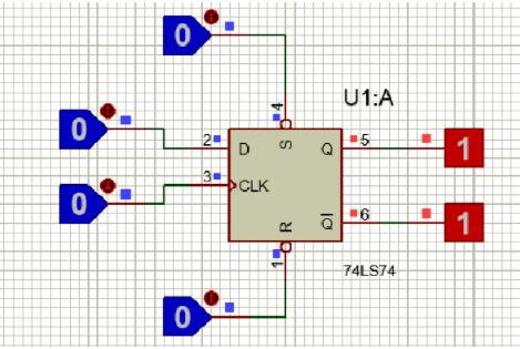
You can also run a simulation of the IC to see if it performs as expected. I've used logic state and logic bits to see if the IC works as it should, but you could use actual circuitry from your application to see if it meets your requirements. The gif file below can be compared to the truth table above to ensure that the IC is functioning properly.
How to use 74LS74