The AD620 Instrumentation Amplifier
Hello everyone, today I will introduce AD620 to you. AD620 is manufactured by Analog Devices. This article is about AD620 pinout, schematic, price and so on. Hope you will enjoy reading it. Now, let's start!

IC INST AMP 1 CIRCUIT 8DIP Hello everyone, today I will introduce AD620 to you.
514
Jul 28, 2021
Michael Eipstein
The AD620 Instrumentation Amplifier
Hello everyone, today I will introduce AD620 to you. AD620 is manufactured by Analog Devices. This article is about AD620 pinout, schematic, price and so on. Hope you will enjoy reading it. Now, let's start!
AD620BN
The AD620 is a low cost, high accuracy instrumentation amplifier that the gain can be adjusted up to 10,000 by the incorporation of only a single resistor. Furthermore, the AD620 features 8-lead SOIC and DIP packaging that is smaller than discrete designs and offers lower power (maximum supply current can merely be around 1.3mA), making it a good fit for battery-powered, portable (or remote) applications.
The AD620, with its high accuracy of 40 ppm maximum nonlinearity, low offset voltage of 50 μV max, and offset drift of 0.6 μV/°C max, is ideal for use in precision data acquisition systems, such as weigh scales and transducer interfaces. Furthermore, Low noise and very low value of input bias current render its suitability for medical devices. such as ECG and noninvasive blood pressure monitors.
The low input bias current of 1.0 nA max is made possible with the use of Superϐeta processing in the input stage. The AD620 works well as a preamplifier due to its low input voltage noise of 9 nV/√Hz at 1 kHz, 0.28 μV p-p in the 0.1 Hz to 10 Hz band,
and 0.1 pA/√Hz input current noise. Also, the AD620 is well suited for multiplexed applications with its settling time of 15 μs to 0.01%, and its cost is low enough to enable designs with one in-amp per channel.
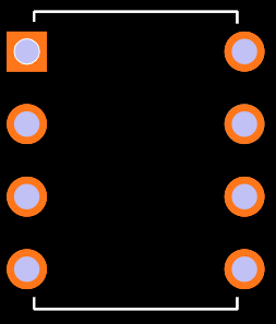
Footprint
★ Easy to use
★ Gain set with one external resistor (Gain range 1 to 10,000)
★ Wide power supply range (±2.3 V to ±18 V)
★ Higher performance than 3 op amp IA designs
★ Available in 8-lead DIP and SOIC packaging
★ Low power, 1.3 mA max supply current
★ Excellent dc performance (B grade)
★ Input Offset Voltage: 50 μV
★ Input Offset Drift: 0.6 μV/°C
★ Input Bias Current: 1.0 nA max
★ 100 dB min common-mode rejection ratio (G = 10) Low noise
★ 9 nV/√Hz @ 1 kHz, input voltage noise
★ 0.28 μV p-p noise (0.1 Hz to 10 Hz)
★ Excellent ac specifications
★ Bandwidth:120 kHz (G = 100)
★ 15 μs settling time to 0.01%
Analog Devices Inc. AD620BN technical specifications, attributes, parameters and parts with similar specifications to Analog Devices Inc. AD620BN.
Analog Devices Inc. AD620BN technical specifications, attributes, parameters and parts with similar specifications to Analog Devices Inc. AD620BN.
| Product Attribute | Attribute Value | |
|---|---|---|
| Contact Plating | Lead, Tin | |
| Mount | Through Hole | |
| Mounting Type | Through Hole | |
| Package / Case | 8-DIP (0.300, 7.62mm) | |
| Number of Pins | 8Pins | |
| Current - Supply (Nom) | 1.3mA | |
| Number of Elements | 1 Element | |
| Operating Temperature | -40°C~85°C | |
| Packaging | Tube | |
| JESD-609 Code | e0 | |
| Pbfree Code | no | |
| Part Status | Obsolete | |
| Moisture Sensitivity Level (MSL) | 1 (Unlimited) | |
| Number of Terminations | 8Terminations | |
| ECCN Code | EAR99 |
| Product Attribute | Attribute Value | |
|---|---|---|
| Resistance | 10GOhm | |
| Max Power Dissipation | 650mW | |
| Voltage - Supply | 36V | |
| Terminal Position | DUAL | |
| Number of Functions | 1Function | |
| Terminal Pitch | 2.54mm | |
| Base Part Number | AD620 | |
| Power Dissipation | 650mW | |
| Current - Supply | 1.3mA | |
| Slew Rate | 1.2V/μs | |
| Amplifier Type | Instrumentation | |
| Common Mode Rejection Ratio | 93 dB | |
| Current - Input Bias | 500pA | |
| Voltage - Supply, Single/Dual (±) | 4.6V~36V ±2.3V~18V | |
| Output Current per Channel | 18mA |
| Product Attribute | Attribute Value | |
|---|---|---|
| Input Offset Voltage (Vos) | 30mV | |
| Neg Supply Voltage-Nom (Vsup) | -15V | |
| Voltage - Input Offset | 15μV | |
| -3db Bandwidth | 1MHz | |
| Input Offset Current-Max (IIO) | 0.00075μA | |
| Voltage Gain-Min | 1 | |
| Voltage Gain-Nom | 10 | |
| Non-linearity-Max | 0.004% | |
| Length | 9.27mm | |
| Height Seated (Max) | 4.57mm | |
| Radiation Hardening | No | |
| RoHS Status | Non-RoHS Compliant | |
| Lead Free | Contains Lead |
The AD620, with its high accuracy of 40 ppm maximum nonlinearity, low offset voltage of 50 μV max, and offset drift of 0.6 μV/°C max, is ideal for use in precision data acquisition systems, such as weigh scales and transducer interfaces. Furthermore, the low noise, low input bias current, and low power of the AD620 make it well suited for medical applications, such as ECG and non-invasive blood pressure monitors.
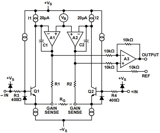
The AD620 only requires a resistor to sets its gain value and hence can be easily set up. A very basic commonly used circuit for AD620 is shown below.

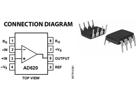
The IC is powered using the pin 7 and pin 4 is connected to ground. Here I have used a singly supply of +5V. The non - inverting pin (pin 2) and the inverting pin (pin 3) is connected the signal which has to be amplified or compared base on the application of the Op-Amp. The Reference pin (pin 5) is normally grounded along with pin 4, the reference pin is used to direct the output towards a voltage when the difference voltage between the inverting and the non-inverting pin is 0V.
The Gain of an Op-Amp can be set by simply connecting the right value of resistor across the pin +Rg (pin 8) and the pin –Rg (pin 1). Here I have connected a resistor of value 500Ω which will set the Op-Amp at a gain value of 100. The formulae to calculate the value of gain from R is given below
G = (49.4 kΏ / RG) + 1
★ Transducer interface
★ Data acquisition systems
★ Industrial process controls
★ Blood Pressure Monitor
★ Medical ECG
★ Weigh Scales
★ Battery operated and portable Devices

ADI (NASDAQ: ADI) is the world leader in the design, manufacture and marketing of a broad portfolio of high-performance analog, mixed-signal, and digital signal processing (DSP) integrated circuits (IC) electronic devices. Since our establishment in 1965, we have been focusing on solving engineering challenges related to signal processing in electronic equipment. Our signal processing products are used by more than 100,000 customers around the world, and play an important role in converting, regulating and processing real-world phenomena such as temperature, pressure, sound, light, speed and motion into electrical signals for use in a wide array of Electronic equipment.
Download datasheets and manufacturer documentation for Analog Devices Inc. AD620BN.
Download datasheets and manufacturer documentation for AD620BN
TAGS
Comments