ATTENTION: Due to increased demand and order volume, processing time may take an additional 1-3 business days.
HomeCommunitySubjectAD845 Op-Amp: Datasheet, Pinout, and AD845 vs. AD744

AD845 Op-Amp: Datasheet, Pinout, and AD845 vs. AD744

Linear - Amplifiers - Instrumentation, OP Amps, Buffer Amps 8-DIP (0.300, 7.62mm) J-FET 15V 0°C~70°C AD845 2.54mm OP AMP, FET FAST SETTLING, DIP, 845

711

Oct 10, 2021

Perry Burke

Linear - Amplifiers - Instrumentation, OP Amps, Buffer Amps 8-DIP (0.300, 7.62mm) J-FET 15V 0°C~70°C AD845 2.54mm OP AMP, FET FAST SETTLING, DIP, 845

The AD845 is a fast, precise, N channel JFET input, monolithic operational amplifier. there is a huge range of Semiconductors, Capacitors, Resistors and ICs in stock. Welcome RFQ.

AD845JNZ

3000In Stock
Min.: 1 Mult.: 1
Quantity Unit Price Ext. Price
1+ $18.46788$18.47
10+ $17.42253$174.23
100+ $16.43635$1643.64
500+ $15.50599$7753
1000+ $14.62829$14628.29
Unit Price:$18.46788
Subtotal: $18.47
Looking for a better price? Want a lower wholesale price? Please send an RFQ, and we will respond immediately.
Quick Links

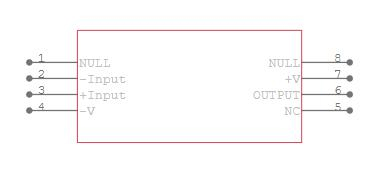
AD845 Pinout

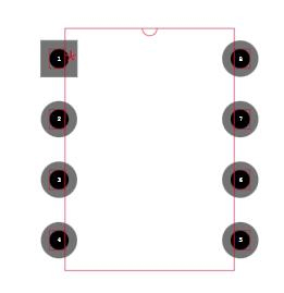
AD845 CAD Model

AD845 Symbol


AD845 Footprint


AD845 3D Model

AD845 Description

The AD845 is a fast, precise, N channel JFET input, monolithicoperational amplifier. It is fabricated using Analog Devices’ complementary bipolar (CB) process. It can easily be used to upgrade many existing designs that use BiFET or FET input hybrid amplifiers and, in some cases, those which use bipolar input op-amps.

Specifications

AD845JNZ Tech Specifications

Analog Devices Inc. AD845JNZ technical specifications, attributes, parameters and parts with similar specifications to Analog Devices Inc. AD845JNZ.

Product Attribute Attribute Value
Lifecycle StatusPRODUCTION (Last Updated: 3 months ago)
Factory Lead Time8 Weeks
Contact PlatingTin
MountThrough Hole
Mounting TypeThrough Hole
Package / Case8-DIP (0.300, 7.62mm)
Number of Pins8Pins
Operating Temperature0°C~70°C
PackagingTube
JESD-609 Codee3
Pbfree Codeno
Part StatusActive
Moisture Sensitivity Level (MSL)1 (Unlimited)
Number of Terminations8Terminations
ECCN CodeEAR99
Max Power Dissipation1.6W
Number of Functions1Function
Supply Voltage15V
Terminal Pitch2.54mm
Product Attribute Attribute Value
Base Part NumberAD845
Pin Count8
Number of Channels1Channel
Operating Supply Current10mA
Nominal Supply Current10mA
Power Dissipation1.6W
Output Current50mA
Quiescent Current10mA
Slew Rate100V/μs
ArchitectureVOLTAGE-FEEDBACK
Amplifier TypeJ-FET
Common Mode Rejection Ratio110 dB
Current - Input Bias750pA
Max Input Voltage18V
Voltage - Supply, Single/Dual (±)±4.75V~18V
Output Current per Channel50mA
Supply TypeDual
Input Offset Voltage (Vos)250μV
Neg Supply Voltage-Nom (Vsup)-15V
Product Attribute Attribute Value
Unity Gain BW-Nom16000 kHz
Voltage Gain113.98dB
Average Bias Current-Max (IIB)0.045μA
Power Supply Rejection Ratio (PSRR)110dB
Low-OffsetNO
Frequency CompensationYES
Voltage - Input Offset700μV
Bias Current-Max (IIB) @25C0.002μA
Dual Supply Voltage15V
Input Capacitance4pF
Height3.43mm
Length9.27mm
Width7.24mm
REACH SVHCNo SVHC
Radiation HardeningNo
RoHS StatusROHS3 Compliant
Lead FreeContains Lead
0 Products View Similar

AD845 Features

• Replaces Hybrid Amplifiers in Many Applications
• AC PERFORMANCE:
- Settles to 0.01% in 350 ns
- 100 V/s Slew Rate
- 12.8 MHz Min Unity Gain Bandwidth
- 1.75 MHz Full Power Bandwidth at 20 V p-p
• DC PERFORMANCE:
- 0.25 mV Max Input Offset Voltage
- 5 V/C Max Offset Voltage Drift
- 0.5 nA Input Bias Current
- 250 V/mV Min Open-Loop Gain
- 4 V p-p Max Voltage Noise, 0.1 Hz to 10 Hz
- 94 dB Min CMRR
• Available in Plastic Mini-DIP, Hermetic CERDIP, and SOIC Packages. Also Available in Tape and Reel in Accordance with EIA-481A Standard

AD845 Application

  • Active filters

  • High-speed integrators

  • Photodiode preamps

  • Sample-and-hold amplifiers

  • Log amplifiers

  • For buffering A/D and D/A converters

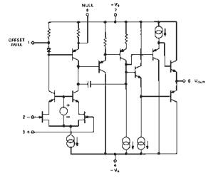
AD845 Simplified Schematic

AD845 Simplified Schematic

How AD845 Driving the Analog Input of an A/D Converter

The circuit below shows an op-amp controlling the analogue input of an A/D converter. It must be able to maintain a constant output voltage under dynamically changing load conditions. The input current is compared to a sequence of switched trial currents in consecutive approximation converters. The comparison point is diode clamped, however, it can stray several hundred millivolts, resulting in A/D input current modulation at a high frequency. The loop gain artificially lowers the output impedance of a feedback amplifier. The amplifier output impedance can approach its open-loop value at high frequencies where the loop gain is low.
AD845 As ADC Unity Gain Buffer

Due to current limiting resistors, most IC amplifiers have a minimum open-loop output impedance of 25 W. A few hundred microamps reflected from converter loading changes can cause sudden input voltage errors. The amplifier's output will recover to the nominal value before the converter makes its comparison if the A/D conversion speed is not excessive and the amplifier's bandwidth is sufficient. However, many amplifiers have a narrow bandwidth, resulting in delayed output transient recovery.

Because it has a wide bandwidth and a high open-loop gain, the AD845 is appropriate for driving high-resolution A/D converters with conversion periods of 5 ms or more.

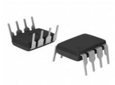
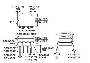
AD845 Package

AD845 Manufacturer

Analog Devices is an international market leader in the design, production, and commercialization of a large range of high-performance integrated circuits (ICs) for analogue, mixed-signal, and digital signals (DSP) processing of almost all electronic systems. Since we started in 1965, the focus has been on the engineering challenge in electronic equipment related to signal to process. Our signal processing solutions, utilized by over 100,000 customers worldwide, play a key role in the conversion, conditioning, and processing of real-world events such as temperature, pressure, sonority, illumination, speed, and movement to electric signals for a wide range of electronic devices.

Datasheet PDF

AD845JNZ Documents

Download datasheets and manufacturer documentation for AD845JNZ

Frequently Asked Questions

Does AD845 conforms to the standard op amp pinout?
Yes, the AD845 conforms to the standard op-amp pinout except that offset nulling is to V+.
How does AD845 work?
The 250 mV max input offset voltage makes offset nulling unnecessary in many applications. The common-mode rejection ratio of 110 dB over a ± 10 V input voltage range represents exceptional performance for a JFET input high-speed op-amp. This, together with a minimum open-loop gain of 250 V/mV ensures that 12-bit performance is achieved, even in unity gain buffer circuits.
What package does AD845 come?
The commercial version is available in an 8-lead plastic mini-DIP and 16-lead SOIC; J and S grade chips are also available.
What can I do with the ad845?
The AD845 is ideal for use in applications such as active filters, high-speed integrators, photodiode preamps, sample-and-hold amplifiers, log amplifiers, and buffering A/D and D/A converters. The 250 µV max input offset voltage makes offset nulling unnecessary in many applications.
What is the temperature range of the ad845s?
The AD845S is specified to operate over the full military temperature range of -55°C to +125°C. Both the industrial and military versions are available in 8-pin credit packages. The commercial version is available in an 8-pin plastic mini-DIP and 16-pin SOIC; "J" and "S" grade chips are also available.
How does the ad845 conform to the standard op amp pinout?
The AD845 conforms to the standard op-amp pinout except that offset nulling is to V+. The AD845J and AD845K grade devices are available specified to operate over the commercial 0°C to +70°C temperature range. AD845A and AD845B devices are specified for operation over the -40°C to +85°C industrial temperature range.
FAQ
Does AD845 conforms to the standard op amp pinout?
Yes, the AD845 conforms to the standard op-amp pinout except that offset nulling is to V+.
How does AD845 work?
The 250 mV max input offset voltage makes offset nulling unnecessary in many applications. The common-mode rejection ratio of 110 dB over a ± 10 V input voltage range represents exceptional performance for a JFET input high-speed op-amp. This, together with a minimum open-loop gain of 250 V/mV ensures that 12-bit performance is achieved, even in unity gain buffer circuits.
What package does AD845 come?
The commercial version is available in an 8-lead plastic mini-DIP and 16-lead SOIC; J and S grade chips are also available.
What can I do with the ad845?
The AD845 is ideal for use in applications such as active filters, high-speed integrators, photodiode preamps, sample-and-hold amplifiers, log amplifiers, and buffering A/D and D/A converters. The 250 µV max input offset voltage makes offset nulling unnecessary in many applications.
What is the temperature range of the ad845s?
The AD845S is specified to operate over the full military temperature range of -55°C to +125°C. Both the industrial and military versions are available in 8-pin credit packages. The commercial version is available in an 8-pin plastic mini-DIP and 16-pin SOIC; "J" and "S" grade chips are also available.
How does the ad845 conform to the standard op amp pinout?
The AD845 conforms to the standard op-amp pinout except that offset nulling is to V+. The AD845J and AD845K grade devices are available specified to operate over the commercial 0°C to +70°C temperature range. AD845A and AD845B devices are specified for operation over the -40°C to +85°C industrial temperature range.

TAGS

Share