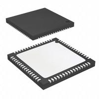
Clock Generator 64-Pin LFCSP EP Tray
The AD9520-0BCPZ is IC CLOCK GEN 2.8GHZ VCO 64LFCSP, which is designed to work as Clock/Timing - Clock Generators, PLLs, Frequency Synthesizers.

Clock Generator 64-Pin LFCSP EP Tray The AD9520-0BCPZ is IC CLOCK GEN 2.8GHZ VCO 64LFCSP, which is designed to work as Clock/Timing - Clock Generators, PLLs, Frequency Synthesizers.
151
Jun 7, 2021
Abbott
Clock Generator 64-Pin LFCSP EP Tray
The AD9520-0BCPZ is IC CLOCK GEN 2.8GHZ VCO 64LFCSP, which is designed to work as Clock/Timing - Clock Generators, PLLs, Frequency Synthesizers.
AD9520-0BCPZ
| Quantity | Unit Price | Ext. Price |
|---|---|---|
| 1+ | $108.14401 | $108.14 |
| 10+ | $102.02265 | $1020.23 |
| 100+ | $96.24778 | $9624.78 |
| 500+ | $90.79979 | $45399.9 |
| 1000+ | $85.66018 | $85660.18 |
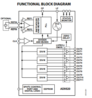
Low phase noise, phase-locked loop (PLL)
On-chip VCO tunes from 2.53 GHz to 2.95 GHz Optional external 3.3 V/5 V VCO/VCXO to 2.4 GHz 1 differential or 2 single-ended reference inputs
Accepts CMOS, LVDS, or LVPECL references to 250 MHz Accepts 16.62 MHz to 33.3 MHz crystal for reference input
Optional reference clock doubler
Reference monitoring capability
Automatic/manual reference holdover and reference switchover modes, with revertive switching Glitch-free switchover between references
Automatic recovery from holdover
Digital or analog lock detect, selectable
Optional zero delay operation
Twelve 1.6 GHz LVPECL outputs divided into 4 groups
Each group of 3 outputs shares a 1-to-32 divider with phase delay
Additive output jitter as low as 225 fs rms
Channel-to-channel skew grouped outputs < 16 ps
Each LVPECL output can be configured as 2 CMOS outputs (for fOUT ≤ 250 MHz)
Automatic synchronization of all outputs on power-up
Manual output synchronization available
SPI- and I²C-compatible serial control port
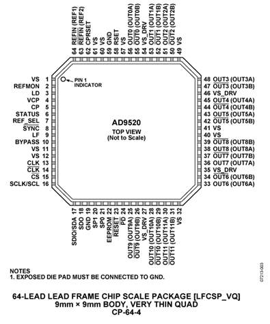
64-lead LFCSP
Nonvolatile EEPROM stores configuration settings
The AD9520-0BCPZ provides a multi-output clock distribution function with subpicosecond jitter performance, along with an on-chip PLL and VCO. The on-chip VCO tunes from 2.53 GHz to 2.95 GHz. An external 3.3 V/5 V VCO/VCXO of up to 2.4 GHz can also be used.
The AD9520-0BCPZ serial interface supports both SPI and I²C ports. An in-package EEPROM, which can be programmed through the serial interface, can store user-defined register settings for power-up and chip reset.
The AD9520-0BCPZ features 12 LVPECL outputs in four groups. Any of the 1.6 GHz LVPECL outputs can be reconfigured as two 250 MHz CMOS outputs. If an application requires LVDS drivers instead of LVPECL drivers, refer to the AD9520-0BCPZ.
Each group of three outputs has a divider that allows both the divide ratio (from 1 to 32) and the phase offset or coarse time delay to be set.
The AD9520-0BCPZ is available in a 64-lead LFCSP and can be operated from a single 3.3 V supply. The external VCO can have an operating voltage of up to 5.5 V. A separate output driver power supply can be from 2.375 V to 3.465 V.
The AD9520-0BCPZ is specified for operation over the standard industrial range of −40°C to +85°C.
Analog Devices Inc. AD9520-0BCPZ technical specifications, attributes, parameters and parts with similar specifications to Analog Devices Inc. AD9520-0BCPZ.
Analog Devices Inc. AD9520-0BCPZ technical specifications, attributes, parameters and parts with similar specifications to Analog Devices Inc. AD9520-0BCPZ.
| Product Attribute | Attribute Value | |
|---|---|---|
| Factory Lead Time | 8 Weeks | |
| Lifecycle Status | PRODUCTION (Last Updated: 3 weeks ago) | |
| Surface Mount | YES | |
| Package / Case | 64-VFQFN Exposed Pad, CSP | |
| Mounting Type | Surface Mount | |
| Number of Pins | 64Pins | |
| Frequency(Max) | 2.95GHz | |
| Packaging | Tray | |
| Operating Temperature | -40°C~85°C | |
| JESD-609 Code | e3 | |
| Pbfree Code | no | |
| Part Status | Active | |
| Moisture Sensitivity Level (MSL) | 3 (168 Hours) | |
| Number of Terminations | 64Terminations | |
| ECCN Code | EAR99 |
| Product Attribute | Attribute Value | |
|---|---|---|
| Type | Clock Generator, Fanout Distribution | |
| Terminal Finish | Tin (Sn) | |
| Voltage - Supply | 3.135V~3.465V | |
| Terminal Position | QUAD | |
| Terminal Form | NO LEAD | |
| Peak Reflow Temperature (Cel) | 260 | |
| Terminal Pitch | 0.5mm | |
| Frequency | 1.6GHz | |
| Time@Peak Reflow Temperature-Max (s) | 30 | |
| Base Part Number | AD9520 | |
| Output | CMOS, LVPECL | |
| Pin Count | 64 | |
| Number of Outputs | 12Outputs | |
| Qualification Status | Not Qualified | |
| Number of Circuits | 1Circuit |
| Product Attribute | Attribute Value | |
|---|---|---|
| Logic Function | Clock | |
| Input | CMOS, LVDS, LVPECL | |
| Ratio - Input:Output | 2:12, 2:24 | |
| Primary Clock/Crystal Frequency-Nom | 33.33MHz | |
| PLL | Yes | |
| Differential - Input:Output | Yes/Yes | |
| Max Duty Cycle | 50 % | |
| Divider/Multiplier | Yes/No | |
| Width | 9.1mm | |
| Length | 9.1mm | |
| Height | 950μm | |
| RoHS Status | ROHS3 Compliant | |
| REACH SVHC | No SVHC | |
| Lead Free | Contains Lead |
Low jitter, low phase noise clock distribution
Clock generation and translation for SONET, 10Ge, 10GFC, Synchronous Ethernet, OTU2/3/4 Forward error correction (G.710)
Clocking high-speed ADCs, DACs, DDSs, DDCs, DUCs, MxFEs
High-performance wireless transceivers
ATE and high-performance instrumentation
Broadband infrastructures
Analog Devices (NASDAQ: ADI) is a world leader in the design, manufacture, and marketing of a broad portfolio of high performance analog, mixed-signal, and digital signal processing (DSP) integrated circuits (ICs) used in virtually all types of electronic equipment. Since our inception in 1965, we have focused on solving the engineering challenges associated with signal processing in electronic equipment. Used by over 100,000 customers worldwide, our signal processing products play a fundamental role in converting, conditioning, and processing real-world phenomena such as temperature, pressure, sound, light, speed, and motion into electrical signals to be used in a wide array of electronic devices.
Download datasheets and manufacturer documentation for Analog Devices Inc. AD9520-0BCPZ.
Download datasheets and manufacturer documentation for AD9520-0BCPZ
TAGS
Comments