ATTENTION: Due to increased demand and order volume, processing time may take an additional 1-3 business days.
HomeCommunitySubjectADA4610-2 JFET Dual Op-Amp: Pinout, Equivalent and Datasheet

ADA4610-2 JFET Dual Op-Amp: Pinout, Equivalent and Datasheet

Linear - Amplifiers - Instrumentation, OP Amps, Buffer Amps 8-SOIC (0.154, 3.90mm Width) J-FET 5V -40°C~125°C ADA4610 9.5MHz ANALOG DEVICES ADA4610-2ARZOperational Amplifier, Dual, 16.3 MHz, 2 Amplifier, 17 V/s,4.5V to15V, SOIC, 8 Pins

81

Nov 5, 2021

Edith Fowler

JFET Amplifiers - 02 Common Source Amp Configurations


Linear - Amplifiers - Instrumentation, OP Amps, Buffer Amps 8-SOIC (0.154, 3.90mm Width) J-FET 5V -40°C~125°C ADA4610 9.5MHz ANALOG DEVICES ADA4610-2ARZOperational Amplifier, Dual, 16.3 MHz, 2 Amplifier, 17 V/s,4.5V to15V, SOIC, 8 Pins

The ADA4610-2 is precision junction field effect transistor (JFET) amplifier that features low input noise voltage, current noise, offset voltage, input bias current, and rail-to-rail output. The ADA4610-2 is a dual amplifier. Furthermore, Huge range of Semiconductors, Capacitors, Resistors and IcS in stock. Welcome RFQ.
ADA4610-2ARZ

2In Stock
Min.: 1 Mult.: 1
Quantity Unit Price Ext. Price
1+ $5.18298$5.18
10+ $4.8896$48.9
100+ $4.61283$461.28
500+ $4.35173$2175.86
1000+ $4.10541$4105.41
Unit Price:$5.18298
Subtotal: $5.18
Looking for a better price? Want a lower wholesale price? Please send an RFQ, and we will respond immediately.
Quick Links

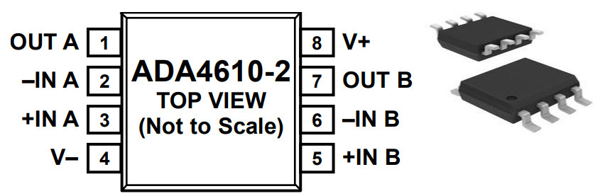
ADA4610-2 Pinout

Pinout

ADA4610-2 Overview

The ADA4610-2 is precision junction field effect transistor (JFET) amplifier that features low input noise voltage, current noise, offset voltage, input bias current, and rail-to-rail output. The ADA4610-2 is a dual amplifier. The ADA4610-2 is specified over the −40°C to +125°C extended industrial temperature range. The ADA4610-2 is available in 8-lead SOIC, 8-lead MSOP, and 8-lead LFCSP packages.

This article provides you with a basic overview of the ADA4610-2 JFET Dual Op Amp, including its pin descriptions, features and specifications, etc., to help you quickly understand what ADA4610-2 is.

ADA4610-2 CAD Model

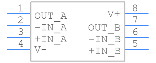
PCB Symbol

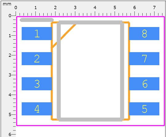
PCB Footprint

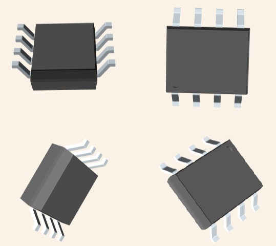
3D Model

ADA4610-2 Features

● Low offset voltage

   ◆ B grade: 0.4 mV maximum

   ◆ A grade: 1 mV maximum

● Low offset voltage drift

   ◆ B grade: 2 µV/°C maximum

   ◆ A grade: 8 µV/°C maximum (SOIC, MSOP, LFCSP packages)

● Low input bias current: 5 pA typical

● Dual-supply operation: ±5 V to ±15 V

● Low voltage noise: 0.45 µV p-p at 0.1 Hz to 10 Hz

● Voltage noise density: 7.30 nV/√Hz at f = 1 kHz

● Low THD + N: 0.00025%

● No phase reversal

● Rail-to-rail output

● Unity-gain stable

● Long-term offset voltage drift (10,000 hours): 5 µV typical

● Temperature hysteresis: 8 µV typical

ADA4610-2 Advantage

The combination of low offset, noise, and very low input bias current makes this amplifier especially suitable for high impedance sensor amplification and precise current measurements using shunts. With excellent dc precision, low noise, and fast settling time, the ADA4610-2 provides superior accuracy in medical instruments, electronic measurement, and automated test equipment. Unlike many competitive amplifiers, the ADA4610-2 maintains fast settling performance with substantial capacitive loads. Unlike many older JFET amplifiers, the ADA4610-2 does not suffer from output phase reversal when input voltages exceed the maximum common-mode voltage range. The fast slew rate and great stability with capacitive loads make the ADA4610-2 ideal for high performance filters. Low input bias currents, low offset, and low noise result in a wide dynamic range for photodiode amplifier circuits. Low noise and distortion, high output current, and excellent speed make the ADA4610-2 great choices for audio applications. 

Specifications

Analog Devices Inc. ADA4610-2ARZ technical specifications, attributes, parameters and parts with similar specifications to Analog Devices Inc. ADA4610-2ARZ.

ADA4610-2ARZ Tech Specifications

Analog Devices Inc. ADA4610-2ARZ technical specifications, attributes, parameters and parts with similar specifications to Analog Devices Inc. ADA4610-2ARZ.

Product Attribute Attribute Value
Lifecycle StatusPRODUCTION (Last Updated: 3 weeks ago)
Factory Lead Time26 Weeks
Mounting TypeSurface Mount
Package / Case8-SOIC (0.154, 3.90mm Width)
Surface MountYES
Number of Pins8Pins
Weight540.001716mg
Operating Temperature-40°C~125°C
PackagingTube
JESD-609 Codee3
Pbfree Codeno
Part StatusActive
Moisture Sensitivity Level (MSL)1 (Unlimited)
Number of Terminations8Terminations
ECCN CodeEAR99
Terminal FinishMatte Tin (Sn)
Terminal PositionDUAL
Terminal FormGULL WING
Peak Reflow Temperature (Cel)260
Product Attribute Attribute Value
Number of Functions2Functions
Supply Voltage5V
Time@Peak Reflow Temperature-Max (s)30
Base Part NumberADA4610
Pin Count8
Output TypeRail-to-Rail
Power Supplies+-4.5/+-15/9/30V
Number of Channels2Channels
Operating Supply Current3mA
Quiescent Current1.6mA
Slew Rate61V/μs
ArchitectureVOLTAGE-FEEDBACK
Amplifier TypeJ-FET
Common Mode Rejection Ratio115 dB
Current - Input Bias5pA
Voltage - Supply, Single/Dual (±)±4.5V~15V
Output Current per Channel79mA
Input Offset Voltage (Vos)400μV
Bandwidth16.3MHz
Product Attribute Attribute Value
Neg Supply Voltage-Nom (Vsup)-5V
Unity Gain BW-Nom15400 kHz
Voltage Gain100dB
Average Bias Current-Max (IIB)0.0015μA
Power Supply Rejection Ratio (PSRR)125dB
Low-OffsetNO
Frequency CompensationYES
Low-BiasYES
-3db Bandwidth9.5MHz
Input Voltage Noise Density14nV/sqrt Hz
Height1.05mm
Length5.1mm
Width4.5mm
REACH SVHCNo SVHC
Radiation HardeningNo
RoHS StatusROHS3 Compliant
Lead FreeContains Lead
0 Products View Similar

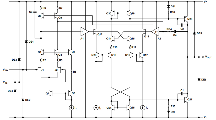
ADA4610-2 Functional Block Diagram

Simplified Schematic

ADA4610-2 Equivalent

          Model number                Manufacturer                                               Description
ADA4610-2ARZ-RL Analog Devices Inc Low Noise, Precision, Rail-to-Rail Output, JFET Dual Op Amp
ADA4610-2ARZ-R7 Analog Devices Inc Low Noise, Precision, Rail-to-Rail Output, JFET Dual Op Amp
ADA4610-2ARMZ-RL Analog Devices Inc Low Noise, Precision, Rail-to-Rail Output, JFET Dual Op Amp
ADA4610-2ARMZ-R7 Analog Devices Inc Low Noise, Precision, Rail-to-Rail Output, JFET Dual Op Amp
ADA4610-2ACPZ-RL Analog Devices Inc Low Noise, Precision, Rail-to-Rail Output, JFET Dual Op Amp

ADA4610-2 Application

● Instrumentation

● Medical instruments

● Multipole filters

● Precision current measurement

● Photodiode amplifiers

● Sensors

● Audio

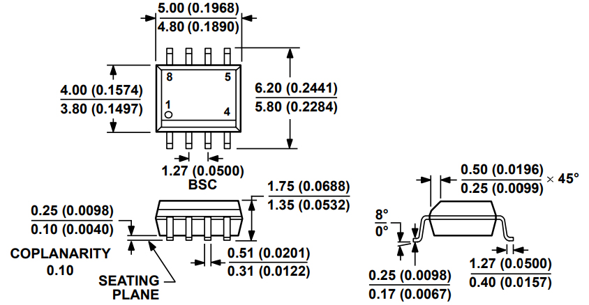
ADA4610-2 Package

8-Lead Standard Small Outline Package

ADA4610-2 Manufacturer

Analog Devices (NASDAQ: ADI) is a world leader in the design, manufacture, and marketing of a broad portfolio of high performance analog, mixed-signal, and digital signal processing (DSP) integrated circuits (ICs) used in virtually all types of electronic equipment. Since our inception in 1965, we have focused on solving the engineering challenges associated with signal processing in electronic equipment. Used by over 100,000 customers worldwide, our signal processing products play a fundamental role in converting, conditioning, and processing real-world phenomena such as temperature, pressure, sound, light, speed, and motion into electrical signals to be used in a wide array of electronic devices.

Datasheet PDF

ADA4610-2ARZ Documents

Download datasheets and manufacturer documentation for ADA4610-2ARZ

Frequently Asked Questions

Can ADA4610-2 allow higher voltage than the supply to be applied to the input without damage?
The ADA4610-2 has internal protective circuitry that allows voltages as high as 0.3 V beyond the supplies to be applied at the input of either terminal without causing damage.
Can ADA4610-2 reduce excess supply current?
The ADA4610-2 has a unique output stage design that reduces the excess supply current but does not entirely eliminate this effect when the op amp is operating in open-loop mode.
Can the ADA4610-2 combine high precision and high speed characteristics into a high voltage, low power op amp?
The unique architecture of the ADA4610-2 makes it possible to combine high precision and high speed characteristics into a high voltage, low power op amp.
What is the extended industrial temperature range and supply voltages of the ADA4610-2?
The ADA4610-2 is fully specified with supply voltages from ±5 V to ±15 V over the extended industrial temperature range of −40°C to +125°C.
FAQ
Can ADA4610-2 allow higher voltage than the supply to be applied to the input without damage?
The ADA4610-2 has internal protective circuitry that allows voltages as high as 0.3 V beyond the supplies to be applied at the input of either terminal without causing damage.
Can ADA4610-2 reduce excess supply current?
The ADA4610-2 has a unique output stage design that reduces the excess supply current but does not entirely eliminate this effect when the op amp is operating in open-loop mode.
Can the ADA4610-2 combine high precision and high speed characteristics into a high voltage, low power op amp?
The unique architecture of the ADA4610-2 makes it possible to combine high precision and high speed characteristics into a high voltage, low power op amp.
What is the extended industrial temperature range and supply voltages of the ADA4610-2?
The ADA4610-2 is fully specified with supply voltages from ±5 V to ±15 V over the extended industrial temperature range of −40°C to +125°C.

TAGS

Share