ATTENTION: Due to increased demand and order volume, processing time may take an additional 1-3 business days.
HomeCommunitySubjectADA4622-4 Precision Op-Amp: Features, Pinout and Datasheet

ADA4622-4 Precision Op-Amp: Features, Pinout and Datasheet

Linear - Amplifiers - Instrumentation, OP Amps, Buffer Amps 14-SOIC (0.154, 3.90mm Width) J-FET 15V -40°C~125°C ADA4622 1.27mm 15.5MHz IC OPAMP JFET 4 CIRCUIT 14SOIC

499

Nov 8, 2021

Tess Morley

What does precision mean for an op amp?


Linear - Amplifiers - Instrumentation, OP Amps, Buffer Amps 14-SOIC (0.154, 3.90mm Width) J-FET 15V -40°C~125°C ADA4622 1.27mm 15.5MHz IC OPAMP JFET 4 CIRCUIT 14SOIC

The ADA4622-4 is the next generation of the AD824 single-supply, rail-to-rail output (RRO), precision junction field effect transistors (JFET) input op amp. Furthermore, Huge range of Semiconductors, Capacitors, Resistors and IcS in stock. Welcome RFQ.
ADA4622-4ARZ

3635In Stock
Min.: 1 Mult.: 1
Quantity Unit Price Ext. Price
1+ $10.62187$10.62
10+ $10.02063$100.21
100+ $9.45343$945.34
500+ $8.91833$4459.17
1000+ $8.41352$8413.52
Unit Price:$10.62187
Subtotal: $10.62
Looking for a better price? Want a lower wholesale price? Please send an RFQ, and we will respond immediately.
Quick Links

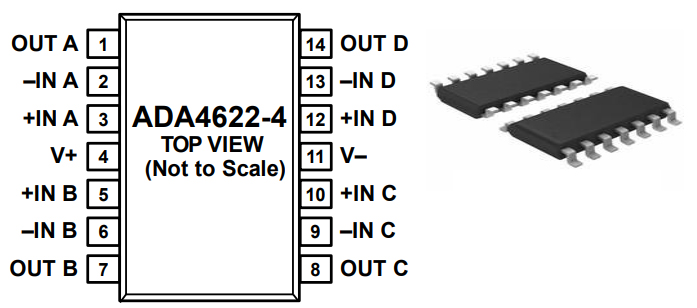
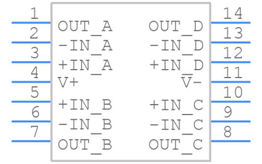
ADA4622-4 Pinout

            Pin No.                      Mnemonic                                                    Description
1 OUT A Output, Channel A.
2 −IN A Inverting Input, Channel A.
3 +IN A Noninverting Input, Channel A.
4 V+ Positive Supply Voltage.
5 +IN B Noninverting Input, Channel B.
6 −IN B Inverting Input, Channel B.
7 OUT B Output, Channel B.
8 OUT C Output, Channel C.
9 −IN C Inverting Input, Channel C.
10 +IN C Noninverting Input, Channel C.
11 V− Negative Supply Voltage.
12 +IN D Noninverting Input, Channel D.
13 −IN D Inverting Input, Channel D.
14 OUT D Output, Channel D.

ADA4622-4 CAD Model

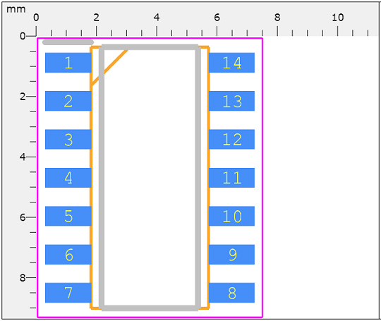
PCB Symbol

PCB Footprint

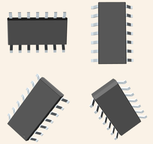
3D Model

ADA4622-4 Overview

The ADA4622-4 is the next generation of the AD824 single-supply, rail-to-rail output (RRO), precision junction field effect transistors (JFET) input op amp. The ADA4622-4 includes many improvements that make it desirable as upgrades without compromising the flexibility and ease of use that makes the AD824 useful for a wide variety of applications. The ADA4622-4 is specified for operation over the extended industrial temperature range of −40°C to +125°C, and operate from 5 V to 30 V, with specifications at +5 V, ±5 V, and ±15 V. The ADA4622-4 is available in a 14-lead SOIC_N and a 16-lead, 4 × 4 mm LFCSP.

This article provides you with a basic overview of the ADA4622-4 Precision Op-Amp, including its pin descriptions, features and specifications, etc., to help you quickly understand what ADA4622-4 is.

ADA4622-4 Features

● Next generation of the AD824

● Wide gain bandwidth product: 8 MHz typical

● High slew rate

   ◆ 23 V/µs typical (low to high)

   ◆ −18 V/µs typical (high to low)

● Low input bias current: ±10 pA maximum at TA = 25°C

● Low offset voltage

   ◆ A grade: ±0.8 mV maximum at T= 25°C

   ◆ B grade: ±0.35 mV maximum at TA = 25°C

● Low offset voltage drift

   ◆ A grade: ±2 µV/°C typical, ±15 µV/°C maximum

   ◆ B grade: ±2 µV/°C typical, ±5 µV/°C maximum

● Input voltage range includes Pin V−

● Rail-to-rail output

● Electromagnetic interference rejection ratio (EMIRR)

   ◆ 90 dB typical at f = 1000 MHz and f = 2400 MHz

● Industry-standard package and pinouts

ADA4622-4 Advantage

The input voltage range includes the negative supply and the output swings rail-to-rail. Input EMI filters increase the signal robustness in the face of closely located switching noise sources. The speed, in terms of bandwidth and slew rate, increases along with a strong output drive to improve settling time performance and enables the devicesto drive the inputs of modern singleended, successive approximation register (SAR) analog-todigital converters (ADCs). Voltage noise is reduced; although the supply current remains the same as the AD824, broadband noise is reduced by 25%, and 1/f is reduced by half. DC precision in the ADA4622-4 improved from the AD824 with half the offset and a maximum thermal drift specification added to the ADA4622-4. The common-mode rejection ratio (CMRR) is improved from the AD824 to make the ADA4622-4 more suitable when used in noninverting gain and difference amplifier configurations.

Specifications

Analog Devices Inc. ADA4622-4ARZ technical specifications, attributes, parameters and parts with similar specifications to Analog Devices Inc. ADA4622-4ARZ.

ADA4622-4ARZ Tech Specifications

Analog Devices Inc. ADA4622-4ARZ technical specifications, attributes, parameters and parts with similar specifications to Analog Devices Inc. ADA4622-4ARZ.

Product Attribute Attribute Value
Lifecycle StatusPRODUCTION (Last Updated: 1 month ago)
Factory Lead Time8 Weeks
Mounting TypeSurface Mount
Package / Case14-SOIC (0.154, 3.90mm Width)
Surface MountYES
Number of Pins14Pins
Operating Temperature-40°C~125°C
PackagingTube
Pbfree Codeno
Part StatusActive
Moisture Sensitivity Level (MSL)1 (Unlimited)
Number of Terminations14Terminations
Terminal PositionDUAL
Terminal FormGULL WING
Product Attribute Attribute Value
Peak Reflow Temperature (Cel)260
Number of Functions4Functions
Supply Voltage15V
Terminal Pitch1.27mm
Time@Peak Reflow Temperature-Max (s)30
Base Part NumberADA4622
Pin Count14
Output TypeRail-to-Rail
Number of Circuits4Circuits
Current - Supply715μA
Slew Rate23V/μs
Amplifier TypeJ-FET
Common Mode Rejection Ratio100 dB
Current - Input Bias2pA
Product Attribute Attribute Value
Voltage - Supply, Single/Dual (±)4.5V~30V ±5V~15V
Gain Bandwidth Product8MHz
Neg Supply Voltage-Nom (Vsup)-15V
Unity Gain BW-Nom7000 kHz
Average Bias Current-Max (IIB)0.0015μA
Supply Voltage Limit-Max18V
Voltage - Input Offset400μV
-3db Bandwidth15.5MHz
Neg Supply Voltage-Max (Vsup)-18V
Length8.65mm
Height Seated (Max)1.75mm
RoHS StatusROHS3 Compliant
0 Products View Similar

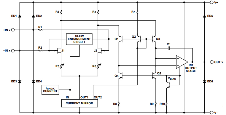
ADA4622-4 Functional Block Diagram

Simplified Circuit Diagram

ADA4622-4 Applications

● High output impedance sensor interfaces

● Photodiode sensor interfaces

● Transimpedance amplifiers

● ADC drivers

● Precision filters and signal conditioning

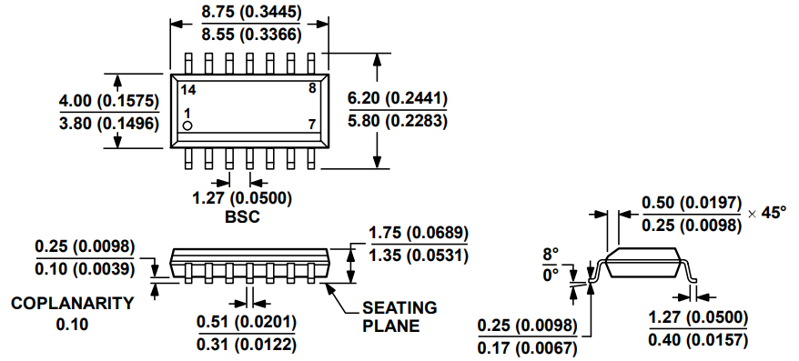
ADA4622-4 Package

14-Lead Standard Small Outline Package [SOIC_N]

ADA4622-4 Manufacturer

Analog Devices (NASDAQ: ADI) is a world leader in the design, manufacture, and marketing of a broad portfolio of high performance analog, mixed-signal, and digital signal processing (DSP) integrated circuits (ICs) used in virtually all types of electronic equipment. Since our inception in 1965, we have focused on solving the engineering challenges associated with signal processing in electronic equipment. Used by over 100,000 customers worldwide, our signal processing products play a fundamental role in converting, conditioning, and processing real-world phenomena such as temperature, pressure, sound, light, speed, and motion into electrical signals to be used in a wide array of electronic devices.

Datasheet PDF

ADA4622-4ARZ Documents

Download datasheets and manufacturer documentation for ADA4622-4ARZ

Frequently Asked Questions

What is the input level of ADA4622-4?
The ADA4622-4 input stage consists of N-channel JFETs that provide low offset, low noise, and high impedance.
How does ADA4622-4 relate to AD824?
The ADA4622-4 is the next generation of the AD824 single-supply, rail-to-rail output (RRO), precision junction field effect transistors (JFET) input op amp. The ADA4622-4 includes many improvements that make it desirable as upgrades without compromising the flexibility and ease of use that makes the AD824 useful for a wide variety of applications.
Does ADA4622-4 have an internal protection circuit? If the overvoltage lasts for more than a few seconds, will the amplifier be damaged?
The ADA4622-4 has internal protective circuitry that allows voltages as high as 0.3 V beyond the supplies applied at the input of either terminal without causing damage. Use a current-limiting resistor in series with the input of the ADA4622-4 if the input voltage exceeds 0.3 V beyond the supply rails of the amplifiers. If the overvoltage condition persists for more than a few seconds, damage to the amplifiers can result.
Can ADA4622-4 be used as a photodiode preamplifier? And if so, what are its advantages?
The ADA4622-4 is an excellent choice for photodiode preamplifier application. The low input bias current minimizes the dc error at the output of the preamplifier. In addition, the high gain bandwidth product and low input capacitance maximizes the signal bandwidth of the photodiode preamplifier.
FAQ
What is the input level of ADA4622-4?
The ADA4622-4 input stage consists of N-channel JFETs that provide low offset, low noise, and high impedance.
How does ADA4622-4 relate to AD824?
The ADA4622-4 is the next generation of the AD824 single-supply, rail-to-rail output (RRO), precision junction field effect transistors (JFET) input op amp. The ADA4622-4 includes many improvements that make it desirable as upgrades without compromising the flexibility and ease of use that makes the AD824 useful for a wide variety of applications.
Does ADA4622-4 have an internal protection circuit? If the overvoltage lasts for more than a few seconds, will the amplifier be damaged?
The ADA4622-4 has internal protective circuitry that allows voltages as high as 0.3 V beyond the supplies applied at the input of either terminal without causing damage. Use a current-limiting resistor in series with the input of the ADA4622-4 if the input voltage exceeds 0.3 V beyond the supply rails of the amplifiers. If the overvoltage condition persists for more than a few seconds, damage to the amplifiers can result.
Can ADA4622-4 be used as a photodiode preamplifier? And if so, what are its advantages?
The ADA4622-4 is an excellent choice for photodiode preamplifier application. The low input bias current minimizes the dc error at the output of the preamplifier. In addition, the high gain bandwidth product and low input capacitance maximizes the signal bandwidth of the photodiode preamplifier.

TAGS

Share