ATTENTION: Due to increased demand and order volume, processing time may take an additional 1-3 business days.
HomeCommunitySubjectADC0804 ADC: Datasheet, Schematic, Pinout

ADC0804 ADC: Datasheet, Schematic, Pinout

IC ADC 8BIT SAR 20DIP The ADC0804 is CMOS 8-bit successive Interfacing Logic Needed – Access Time 135 ns approximation converter (ADC). This post will unlock more details about ADC0804. Furthermore, huge range of Semiconductors, Capacitors, Resistors and ICs in stock. Welcome RFQ.

476

Sep 18, 2021

Maggie Judson

How To Make Analog to Digital VOLTAGE Converter through ADC 0804 IC || ADC Voltage Converter || Easy


IC ADC 8BIT SAR 20DIP

The ADC0804 is CMOS 8-bit successive Interfacing Logic Needed – Access Time 135 ns approximation converter (ADC). This post will unlock more details about ADC0804. Furthermore, huge range of Semiconductors, Capacitors, Resistors and ICs in stock. Welcome RFQ.

ADC0804LCN

11In Stock
Min.: 1 Mult.: 1
Price not displayed? Not available to buy online? Please send an RFQ, and we will respond immediately.
Quick Links

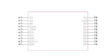
ADC0804 Pinout

ADC0804 Pinout


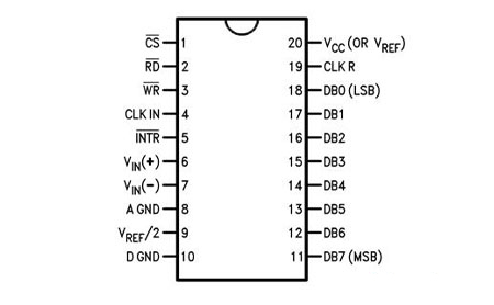
Pin Number Pin Name Description
1 Chip Select (CS) Chip select is used if more than 1 ADC module is used. By default grounded
2 Read (RD) Read pin must be grounded to read the Analog   value
3 Write (WR) Write pin should be pulsed high to start data   conversion
4 CLK IN An external clock can be connected here, else RC   can be used for accessing the internal clock
5 Interrupt (INTR) Goes high for interrupt request.
6 Vin (+) Differential Analog input +. Connect to ADC   input
7 Vin (-) Differential Analog input -. Connect to ground
8 Ground Analog Ground pin connected to the ground of the circuit
9 Vref/2 Reference voltage for ADC conversion.
10 Ground Digital Ground pin connected to the ground of the circuit
11   to 18 Data bit 0 to bit 7 Seven output Data bit pins from which output   is obtained
19 CLK R RC timing resistor input pin for internal   clock gen
20 Vcc Powers the ADC module, use +5V

Pin Description

ADC0804 Description

The ADC0804 is a CMOS 8-Bit, successive approximation A/D converter that uses a modified potentiometric ladder and is designed to operate with the 8080A control bus via three-state outputs. These converters appear to the processor as memory locations or I/O ports, and hence no interfacing logic is required.


ADC0804 CAD Model

ADC0804 Symbol


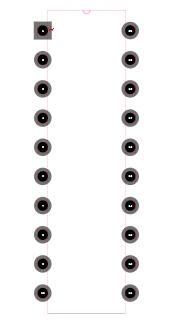
ADC0804 Footprint


ADC0804 3D Model

Specifications

Texas Instruments ADC0804LCN technical specifications, attributes, parameters and parts with similar specifications to Texas Instruments ADC0804LCN.

ADC0804LCN Tech Specifications

Texas Instruments ADC0804LCN technical specifications, attributes, parameters and parts with similar specifications to Texas Instruments ADC0804LCN.

Product Attribute Attribute Value
MountThrough Hole
Mounting TypeThrough Hole
Package / Case20-DIP (0.300, 7.62mm)
Number of Pins20Pins
Operating Temperature0°C~70°C
PackagingTube
JESD-609 Codee0
Part StatusObsolete
Moisture Sensitivity Level (MSL)1 (Unlimited)
Number of Terminations20Terminations
ECCN CodeEAR99
Terminal FinishTin/Lead (Sn/Pb)
Max Power Dissipation875mW
Terminal PositionDUAL
Number of Functions1Function
Supply Voltage5V
Terminal Pitch2.54mm
Product Attribute Attribute Value
Base Part NumberADC0804
Pin Count20
Operating Supply Voltage5V
PolarityUnipolar
Power Supplies5V
ConfigurationADC
Number of Channels1Channel
Max Supply Voltage6.3V
Min Supply Voltage4.5V
Power Dissipation875mW
Number of Bits8Bits
Input TypeDifferential
ArchitectureSAR
Supply TypeSingle
Reference TypeExternal, Supply
Data InterfaceParallel
Resolution1 B
Product Attribute Attribute Value
Sampling Rate10 ksps
Voltage - Supply, Analog4.5V~6.3V
Voltage - Supply, Digital4.5V~6.3V
Number of Analog In Channels1Analog In Channel
Sampling Rate (Per Second)10k
Output Bit CodeBINARY
Power Consumption5.5mW
Linearity Error-Max (EL)0.3906%
Conversion Rate10 ksps
Height3.3mm
Length26.42mm
Width6.6mm
REACH SVHCNo SVHC
Radiation HardeningNo
RoHS StatusNon-RoHS Compliant
Lead FreeContains Lead
0 Products View Similar

ADC0804 Feature

  • Easy to interface with all Microprocessors or works Stand-alone.

  • The single-channel 8-bit ADC module

  • On-chip Clock available, no need for external Oscillator(Clock)

  • Digital output various from 0 to 255

  • When Vref = 5V, for every 19.53mV of analogue value there will be the rise of one bit on the digital side (Step size)

  • Available in 20-pin PDIP, SOIC packages


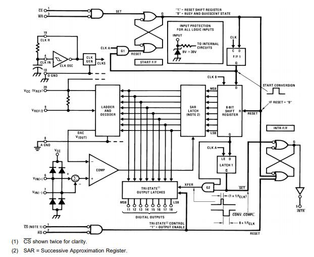
ADC0804 Functional Block Diagram

ADC0804 Functional Block Diagram

ADC0804 Application

• Operates With Any 8-Bit µP Processors or as a Stand-Alone Device

• Interface to Temp Sensors, Voltage Sources, and Transducers

ADC0804 Equivalents

The equivalents for ADC0804: ADC0808, ADC modules.

Where to use ADC0804

The ADC0804 is a commonly used ADC module, for projects where an external ADC is required. It is a 20-pin Single channel 8-bit ADC module. Meaning it can measure one ADC value from 0V to 5V and the precision when voltage reference (Vref –pin 9) is +5V is 19.53mV (Step size). That is for every increase of 19.53mV on the input side there will be an increase of 1 bit on the output side.


This IC is very Ideal to use with Microprocessors like Raspberry Pi, Beagle bone etc.. Or even to use as a standalone ADC module.

How to use ADC0804

Since the IC comes with an internal clock we do not need many components to make it work. However to make the internal clockwork we have to use an RC circuit. The IC should be powered by +5V and both ground pins should be tied to circuit ground. To design the RC circuit simply use a resistor of value 10k and a capacitor of 100pf (approx) and connect them to CLK R and CLK IN pins as shown in the circuit below. The chip select (CS) and Read (R) pin should also be grounded. The Vref pin is left free because by default without any connection it will be connected to +5V.

The digital output will be obtained from the pins DB0 to DB7 and the analogue voltage should be connected to V in(+) pin as shown in the circuit. Also, note that another end of the voltage source (sensor/module) should also be grounded to the circuit for the ADC conversion to work. Now, for the ADC Conversion to start, we have o make the Write(WR) pin go high momentary this can be done by connecting the pin to the I/O of MPU and toggling it high before every ADC read. Only if this is done the ADC value on the output side will be updated.
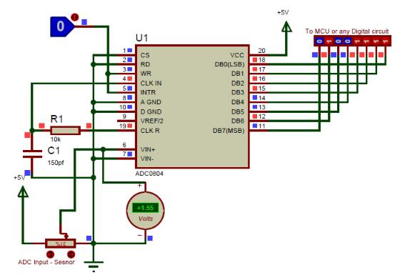
How to use ADC0804

In the above circuit, I have used a potentiometer to feed in a variable voltage of 0V to 5V to the Vin pin and the present Voltage is read using a voltmeter. As you can see in the image the voltage value is 1.55V and the resulting binary value is 01001111. Let us see how this binary value can be converted to an Analog value since we will need it while programming/designing.

 Binary Value = 01001111

 Converting to Decimal  =  (0*128)+(1*64)+(0*32)+(0*16)+(1*8)+(1*4)+(1*2)+(1*1)


                                         =   79


Analog Voltage = Decimal Value * Step size


                             = 79 * 19.53mV


                             = 1.54V


The obtained value is 1.54V and the measured voltage is 1.55V which are very much close. So this is how you use an ADC0804 IC.

 

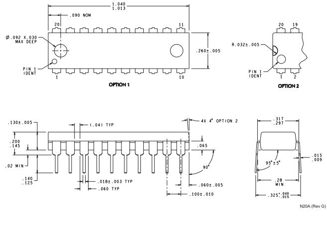
ADC0804 Package

ADC0804 Manufacturer

Texas Instruments (TI) emerges as a globally recognized semiconductor manufacturer expanded into 35 countries. It has seen rapid growth. In 1958, TIer firstly introduced the working integrated circuit. And today more than 30,000 TIers worldwide are committed to designing, manufacturing, and selling analogue and embedded processing chips. They aspire to solve challenges as well as change the world through their technologies.

Datasheet PDF

Download datasheets and manufacturer documentation for Texas Instruments ADC0804LCN.

ADC0804LCN Documents

Download datasheets and manufacturer documentation for ADC0804LCN

Datasheets
ADC0801-05
PCN Obsolescence/ EOL
Mult Devices 06/Nov/2017

Frequently Asked Questions

What is the difference between adc0804 and max1112?
ADC0804 is used for parallel ADC and MAX1112 is used for serial ADC
Which pin of the adc0804 indicates the end of conversion?
PIN-5 – Interrupt (INTR) This pin automatically goes low when the conversion is done by ADC0804 or when the digital equivalent of analogue input is ready. PIN-6 – Vin (+) connect the input analogue sensor pin/input voltage to this pin.
What is the resolution of 8 bit ADC?
For example, an ADC with a resolution of 8 bits can encode an analogue input to one in 256 different levels (28 = 256). The values can represent the ranges from 0 to 255 (i.e. as unsigned integers) or from −128 to 127 (i.e. assigned integer), depending on the application.
FAQ
What is the difference between adc0804 and max1112?
ADC0804 is used for parallel ADC and MAX1112 is used for serial ADC
Which pin of the adc0804 indicates the end of conversion?
PIN-5 – Interrupt (INTR) This pin automatically goes low when the conversion is done by ADC0804 or when the digital equivalent of analogue input is ready. PIN-6 – Vin (+) connect the input analogue sensor pin/input voltage to this pin.
What is the resolution of 8 bit ADC?
For example, an ADC with a resolution of 8 bits can encode an analogue input to one in 256 different levels (28 = 256). The values can represent the ranges from 0 to 255 (i.e. as unsigned integers) or from −128 to 127 (i.e. assigned integer), depending on the application.

TAGS

Share