IC ADC 8BIT SAR 28DIP
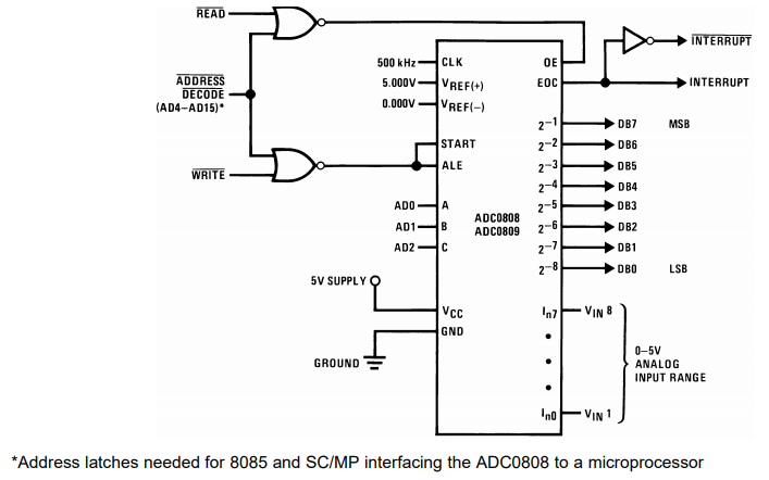
The ADC0809 data acquisition component is a monolithic device with an 8-bit analog-to-digital converter, 8-channel multiplexer, and microprocessor compatible control logic.

IC ADC 8BIT SAR 28DIP The ADC0809 data acquisition component is a monolithic device with an 8-bit analog-to-digital converter,
221
Mar 19, 2021
Ophelia
IC ADC 8BIT SAR 28DIP
The ADC0809 data acquisition component is a monolithic device with an 8-bit analog-to-digital converter, 8-channel multiplexer, and microprocessor compatible control logic.
ADC0809CCN
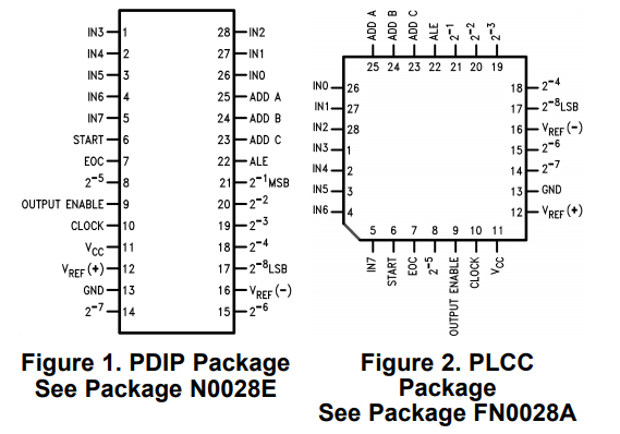
Symbol
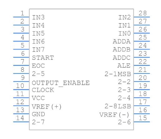
Footprint

3D Model
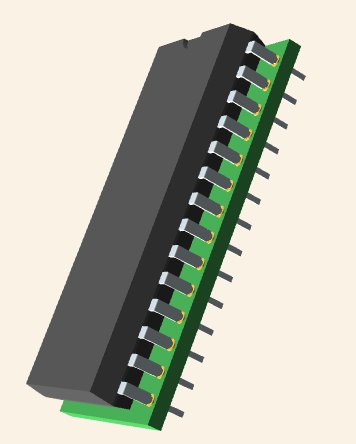
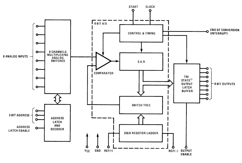
The 8-bit A/D converter uses successive approximation as the conversion technique. The converter features a high impedance chopper stabilized comparator, a 256R voltage divider with an analog switch tree, and a successive approximation register. The 8-channel multiplexer can directly access any of the 8-single-ended analog signals.
The device eliminates the need for external zero to full-scale adjustments. Easy interfacing to microprocessors is provided by the latched and decoded multiplexer address inputs and latched TTL TRI-STATE output.
The design of the ADC0809 has been optimized by incorporating the most desirable aspects of several A/D conversion techniques. The ADC0809 offers high speed, high accuracy, minimal temperature dependence, excellent long-term accuracy and repeatability, and consumes minimal power. These features make this device ideally suited to applications from the process and machine control to consumer and automotive applications. For a 16-channel multiplexer with common output (sample/hold port) see ADC0816 datasheet.
Easy Interface to All Microprocessors
Operates Ratiometrically or with 5 VDC or Analog Span Adjusted Voltage Reference
No Zero or Full-Scale Adjust Required
8-Channel Multiplexer with Address Logic
0V to VCC Input Range
Outputs meet TTL Voltage Level Specifications
ADC0808 Equivalent to MM74C949
ADC0809 Equivalent to MM74C949-1
High speed
High accuracy
Minimal temperature dependence
Excellent long-term accuracy and repeatability
Minimal power consumption
Texas Instruments ADC0809CCN technical specifications, attributes, parameters and parts with similar specifications to Texas Instruments ADC0809CCN.
Texas Instruments ADC0809CCN technical specifications, attributes, parameters and parts with similar specifications to Texas Instruments ADC0809CCN.
| Product Attribute | Attribute Value | |
|---|---|---|
| Contact Plating | Lead, Tin | |
| Mount | Through Hole | |
| Mounting Type | Through Hole | |
| Package / Case | 28-DIP (0.600, 15.24mm) | |
| Number of Pins | 28Pins | |
| Power Dissipation (Max) | 875mW | |
| Current - Supply (Nom) | 300μA | |
| Number of Elements | 1 Element | |
| Operating Temperature | -40°C~85°C | |
| Packaging | Tube | |
| JESD-609 Code | e0 | |
| Part Status | Obsolete | |
| Moisture Sensitivity Level (MSL) | 1 (Unlimited) | |
| Number of Terminations | 28Terminations | |
| ECCN Code | EAR99 | |
| Terminal Finish | Tin/Lead (Sn/Pb) | |
| Voltage - Supply | 5V | |
| Terminal Position | DUAL |
| Product Attribute | Attribute Value | |
|---|---|---|
| Number of Functions | 1Function | |
| Terminal Pitch | 2.54mm | |
| Base Part Number | ADC0809 | |
| Polarity | Unipolar | |
| Power Supplies | 5V | |
| Configuration | MUX-S/H-ADC | |
| Number of Channels | 8Channels | |
| Power Dissipation | 15mW | |
| Number of Bits | 8Bits | |
| Input Type | Single Ended | |
| Architecture | SAR | |
| Converter Type | ADC, SUCCESSIVE APPROXIMATION | |
| Supply Type | Single | |
| Reference Type | External | |
| Data Interface | Parallel | |
| Resolution | 1 B | |
| Sampling Rate | 10 ksps | |
| Voltage - Supply, Analog | 4.5V~6.5V |
| Product Attribute | Attribute Value | |
|---|---|---|
| Voltage - Supply, Digital | 4.5V~6.5V | |
| Number of Analog In Channels | 8Analog In Channels | |
| Sampling Rate (Per Second) | 10k | |
| Output Bit Code | BINARY | |
| Power Consumption | 1.5mW | |
| Sample and Hold / Track and Hold | SAMPLE | |
| Number of A/D Converters | 1A/D Converter | |
| Conversion Rate | 10 ksps | |
| Ratio - S/H:ADC | 1:1 | |
| Voltage - Supply (Max) | 6V | |
| Voltage - Supply (Min) | 4.5V | |
| Height | 3.81mm | |
| Length | 36.83mm | |
| Width | 13.72mm | |
| REACH SVHC | No SVHC | |
| Radiation Hardening | No | |
| RoHS Status | Non-RoHS Compliant | |
| Lead Free | Contains Lead |
As a global semiconductor company operating in 35 countries, Texas Instruments (TI) is first and foremost a reflection of its people. From the TIer who unveiled the first working integrated circuit in 1958 to the more than 30,000 TIers around the world today who design, manufacture, and sell analog and embedded processing chips, we are problem-solvers collaborating to change the world through technology.
Download datasheets and manufacturer documentation for Texas Instruments ADC0809CCN.
Download datasheets and manufacturer documentation for ADC0809CCN
TAGS
Comments