ATTENTION: Due to increased demand and order volume, processing time may take an additional 1-3 business days.
HomeCommunitySubjectADG1419 iCMOS SPDT Switch: Pinout, Features and Datasheet

ADG1419 iCMOS SPDT Switch: Pinout, Features and Datasheet

Interface - Analog Switches, Multiplexers, Demultiplexers 8-WFDFN Exposed Pad, CSP 2.4Ohm -40°C~125°C TA 15V ADG1419 2.4Ohm 0.5mm IC SWITCH SPDT 4.6OHM 8LFCSP

3005

Dec 16, 2021

Tom Bloomer

What is the difference between a SPST, SPDT, DPST, and DPDT switch? - Detailed


Interface - Analog Switches, Multiplexers, Demultiplexers 8-WFDFN Exposed Pad, CSP 2.4Ohm -40°C~125°C TA 15V ADG1419 2.4Ohm 0.5mm IC SWITCH SPDT 4.6OHM 8LFCSP

The ADG1419 is a monolithic iCMOS® device containing a single-pole/double-throw (SPDT) switch. An EN input on the LFCSP is used to enable or disable the device. When disabled, all channels are switched off. The industrial CMOS (iCMOS) modular manufacturing process combines high voltage, complementary metal-oxide semiconductor (CMOS) and bipolar technologies. Furthermore, Huge range of Semiconductors, Capacitors, Resistors and IcS in stock. Welcome RFQ.
ADG1419BCPZ-REEL7

Inquiry
Min.: 1 Mult.: 1
Price not displayed? Not available to buy online? Please send an RFQ, and we will respond immediately.
Quick Links

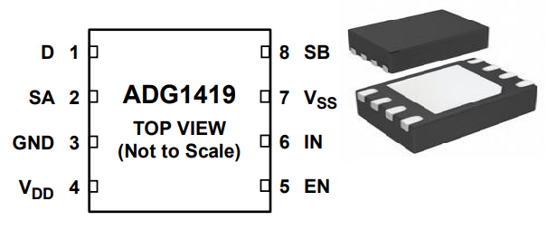
ADG1419 Pinout

The following figure is the diagram of ADG1419 pinout.

Pinout

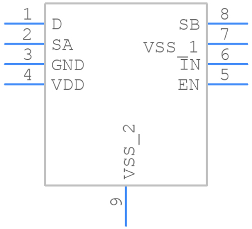
ADG1419 CAD Model

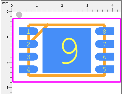
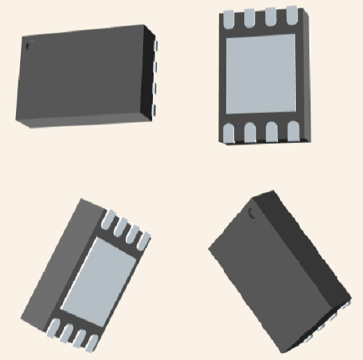
The followings are ADG1419 Symbol, Footprint, and 3D Model.

PCB Symbol


PCB Footprint


3D Model

ADG1419 Overview

The ADG1419 is a monolithic iCMOS® device containing a single-pole/double-throw (SPDT) switch. An EN input on the LFCSP is used to enable or disable the device. When disabled, all channels are switched off. The industrial CMOS (iCMOS) modular manufacturing process combines high voltage, complementary metal-oxide semiconductor (CMOS) and bipolar technologies. It enables the development of a wide range of high performance analog ICs capable of 33 V operation in a footprint that no other generation of high voltage parts has achieved. Unlike analog ICs using conventional CMOS processes, iCMOS components can tolerate high supply voltages while providing increased performance, dramatically lower power consumption, and reduced package size. The on-resistance profile is very flat over the full analog input range, ensuring excellent linearity and low distortion when switching audio signals. The iCMOS construction ensures ultralow power dissipation, making the part ideally suited for portable and battery-powered instruments. Each switch conducts equally well in both directions when on and has an input signal range that extends to the supplies. In the off condition, signal levels up to the supplies are blocked. The ADG1419 exhibits break-before-make switching action for use in multiplexer applications.

This article provides you with a basic overview of the ADG1419 iCMOS SPDT Switch, including its pin descriptions, features and specifications, etc., to help you quickly understand what ADG1419 is.

ADG1419 Features

● 2.1 Ω on resistance

● 0.5 Ω maximum on-resistance flatness at 25°C

● Up to 390 mA continuous current

● Fully specified at +12 V, ±15 V, ±5 V

● No VL supply required

● 3 V logic-compatible inputs

● Rail-to-rail operation

● 8-lead MSOP and 8-lead, 3 mm × 2 mm LFCSP

ADG1419 Product Highlights

● 2.4 Ω maximum on resistance at 25°C.

● Minimum distortion.

● 3 V logic-compatible digital inputs: VINH = 2.0 V, VINL = 0.8 V.

● No VL logic power supply required.

● 8-lead MSOP and 8-lead, 3 mm × 2 mm LFCSP.

Specifications

Analog Devices Inc. ADG1419BCPZ-REEL7 technical specifications, attributes, parameters and parts with similar specifications to Analog Devices Inc. ADG1419BCPZ-REEL7.

ADG1419BCPZ-REEL7 Tech Specifications

Analog Devices Inc. ADG1419BCPZ-REEL7 technical specifications, attributes, parameters and parts with similar specifications to Analog Devices Inc. ADG1419BCPZ-REEL7.

Product Attribute Attribute Value
Factory Lead Time10 Weeks
Lifecycle StatusPRODUCTION (Last Updated: 1 month ago)
Surface MountYES
Package / Case8-WFDFN Exposed Pad, CSP
Mounting TypeSurface Mount
Contact PlatingTin
Number of Pins8Pins
Turn Off Delay Time140 ns
PackagingTape & Reel (TR)
Operating Temperature-40°C~125°C TA
JESD-609 Codee3
Pbfree Codeno
Part StatusActive
Moisture Sensitivity Level (MSL)1 (Unlimited)
Number of Terminations8Terminations
ECCN CodeEAR99
Resistance2.4Ohm
Max Power Dissipation2mW
Terminal PositionBOTTOM
Terminal FormBALL
Peak Reflow Temperature (Cel)260
Number of Functions1Function
Product Attribute Attribute Value
Supply Voltage15V
Terminal Pitch0.5mm
Time@Peak Reflow Temperature-Max (s)40
Base Part NumberADG1419
Pin Count8
Number of Outputs2Outputs
Operating Supply Voltage12V
PolarityNon-Inverting
Number of Channels1Channel
InterfaceParallel
Max Supply Voltage16.5V
Min Supply Voltage5V
Test Frequency1MHz
Power Dissipation2mW
Max Supply Current190μA
Turn On Delay Time110 ns
Number of Inputs1Input
Voltage - Supply, Single/Dual (±)5V~16.5V ±4.5V~16.5V
Supply TypeDual, Single
Bandwidth135MHz
Neg Supply Voltage-Nom (Vsup)-15V
Max Dual Supply Voltage16.5V
Product Attribute Attribute Value
On-State Resistance (Max)2.4Ohm
Min Dual Supply Voltage4.5V
Dual Supply Voltage15V
Multiplexer/Demultiplexer Circuit2:1
Off-state Isolation-Nom64 dB
Current - Leakage (IS(off)) (Max)500pA
Channel Capacitance (CS(off), CD(off))19pF 44pF
On-state Resistance Match-Nom0.05Ohm
Switch CircuitSPDT
Switch Time (Ton, Toff) (Max)110ns, 140ns
Insertion Loss (dB)0.16 dB
Charge Injection-16pC
Channel-to-Channel Matching (ΔRon)50m Ω
SwitchingBREAK-BEFORE-MAKE
Drain to Source Resistance2.4Ohm
Length3mm
RoHS StatusROHS3 Compliant
Radiation HardeningNo
REACH SVHCNo SVHC
Lead FreeContains Lead
0 Products View Similar

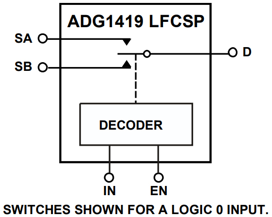
ADG1419 Functional Block Diagram

The following is the Functional Block Diagram of ADG1419.

Functional Block Diagram


ADG1419 Applications

● Automatic test equipment

● Data acquisition systems

● Battery-powered systems

● Relay replacements

● Sample-and-hold systems

● Audio signal routing

● Video signal routing

● Communication systems

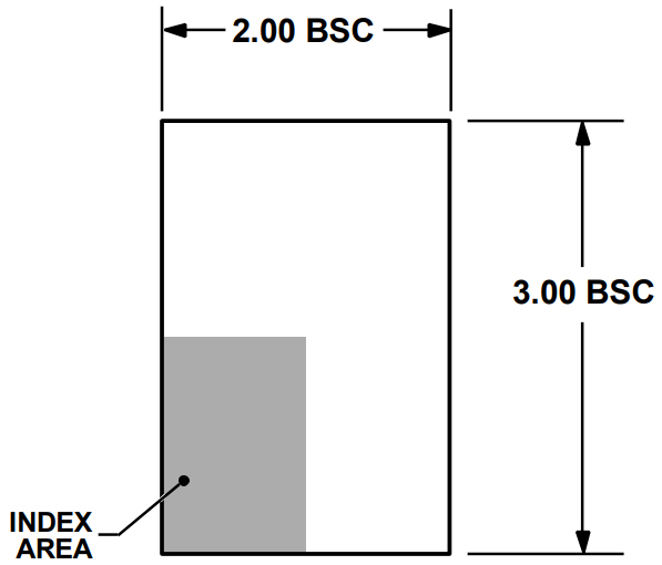
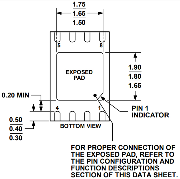
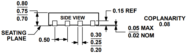
ADG1419 Package

The following diagrams show the ADG1419 package.

Top View


Bottom View


Side View

ADG1419 Manufacturer

Analog Devices (NASDAQ: ADI) is a world leader in the design, manufacture, and marketing of a broad portfolio of high performance analog, mixed-signal, and digital signal processing (DSP) integrated circuits (ICs) used in virtually all types of electronic equipment. Since our inception in 1965, we have focused on solving the engineering challenges associated with signal processing in electronic equipment. Used by over 100,000 customers worldwide, our signal processing products play a fundamental role in converting, conditioning, and processing real-world phenomena such as temperature, pressure, sound, light, speed, and motion into electrical signals to be used in a wide array of electronic devices.

Datasheet PDF

ADG1419BCPZ-REEL7 Documents

Download datasheets and manufacturer documentation for ADG1419BCPZ-REEL7

Frequently Asked Questions

What is the essential property of the ADG1419?
The ADG1419 is a monolithic iCMOS® device containing a single-pole/double-throw (SPDT) switch.
What happens when the ADG1419 is disabled?
When disabled, all channels are switched off.
What is the on-resistance profile of the ADG1419?
The on-resistance profile is very flat over the full analog input range, ensuring excellent linearity and low distortion when switching audio signals.
What does the ADG1419 look like when it's off?
In the off condition, signal levels up to the supplies are blocked.
What does the ADG1419 exhibit for use in multiplexer applications?
The ADG1419 exhibits break-before-make switching action for use in multiplexer applications.
FAQ
What is the essential property of the ADG1419?
The ADG1419 is a monolithic iCMOS® device containing a single-pole/double-throw (SPDT) switch.
What happens when the ADG1419 is disabled?
When disabled, all channels are switched off.
What is the on-resistance profile of the ADG1419?
The on-resistance profile is very flat over the full analog input range, ensuring excellent linearity and low distortion when switching audio signals.
What does the ADG1419 look like when it's off?
In the off condition, signal levels up to the supplies are blocked.
What does the ADG1419 exhibit for use in multiplexer applications?
The ADG1419 exhibits break-before-make switching action for use in multiplexer applications.

TAGS

Share