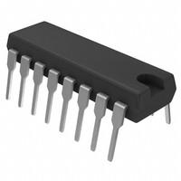
IC MULTIPLEXER 8X1 16DIP
The ADG608BN is monolithic CMOS analog multiplexers comprising eight single channels and four differential channels respectively, fully specified for ±5V, 5V, and 3V power supplies.

IC MULTIPLEXER 8X1 16DIP The ADG608BN is monolithic CMOS analog multiplexers comprising eight single channels and four differential channels respectively, fully specified for ±5V, +5V, and +3V power supplies.
181
Mar 4, 2021
Valerie
IC MULTIPLEXER 8X1 16DIP
The ADG608BN is monolithic CMOS analog multiplexers comprising eight single channels and four differential channels respectively, fully specified for ±5V, 5V, and 3V power supplies.
ADG608BN
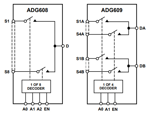
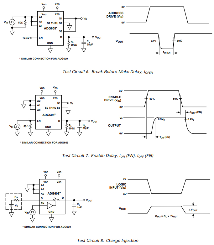
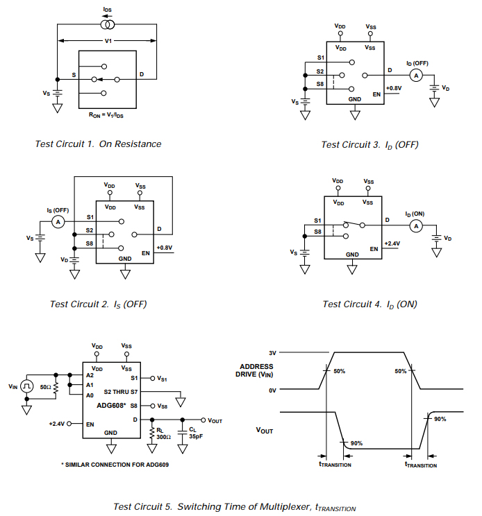
The ADG608BN switches one of eight inputs to a common output as determined by the 3-bit binary address lines A0, A1, and A2. The ADG609 switches one of four differential inputs to a common differential output as determined by the 2-bit binary address lines A0 and A1. An EN input on both devices is used to enable or disable the device. When disabled, all channels are switched OFF. All the address and enable inputs are TTL compatible over the full specified operating temperature range, making the parts suitable for bus-controlled systems such as data acquisition systems, process controls, avionics, and ATEs since the TTL compatible address inputs simplify the digital interface design and reduce the board space requirements. The ADG608/ADG609 are designed on an enhanced LC2 MOS process that provides low power dissipation yet gives high switching speed and low on-resistance. Each channel conducts equally well in both directions when ON and has an input signal range that extends to the supplies. In the OFF condition, signal levels up to the supplies are blocked. All channels exhibit break-before-make switching action preventing momentary shorting when switching channels. Inherent in the design is low charge injection for minimum transients when switching the digital inputs.
+3V, +5V, 65V power supplies
VSS to VDD analog signal range
Low on-resistance (30 V max)
Fast switching times
tON 75ns max
tOFF 45 ns max
Low power dissipation (1.5 mW max)
Break-before-make construction
ESD > 5000V as per ,military standard 3015.7
TTL and CMOS compatible inputs
Automatic test equipment
Data acquisition systems
Communication systems
Avionics and military systems
Microprocessor controlled analog systems
Medical instrumentation
Battery-powered instruments
Remote powered equipment
Compatible with 65V DACs and ADCs such as AD7840/8, AD7870/1/2/4/5/6/8
Analog Devices Inc. ADG608BN technical specifications, attributes, parameters and parts with similar specifications to Analog Devices Inc. ADG608BN.
Analog Devices Inc. ADG608BN technical specifications, attributes, parameters and parts with similar specifications to Analog Devices Inc. ADG608BN.
| Product Attribute | Attribute Value | |
|---|---|---|
| Mounting Type | Through Hole | |
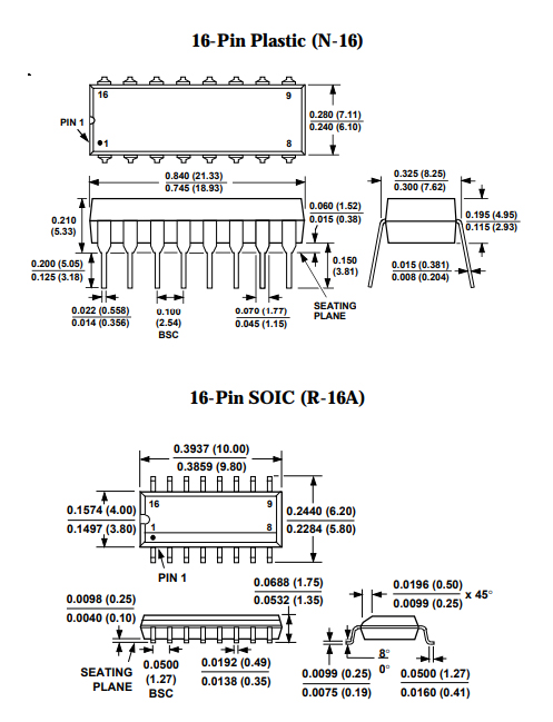
| Package / Case | 16-DIP (0.300, 7.62mm) | |
| Surface Mount | NO | |
| Number of Pins | 16Pins | |
| Operating Temperature | -40°C~85°C TA | |
| Packaging | Tube | |
| JESD-609 Code | e0 | |
| Part Status | Obsolete | |
| Moisture Sensitivity Level (MSL) | 1 (Unlimited) | |
| Number of Terminations | 16Terminations | |
| ECCN Code | EAR99 | |
| Resistance | 30Ohm | |
| Additional Feature | OPERATION WITH SINGLE 3V/5V ALSO POSSIBLE | |
| Voltage - Supply | 5V | |
| Terminal Position | DUAL |
| Product Attribute | Attribute Value | |
|---|---|---|
| Number of Functions | 1Function | |
| Terminal Pitch | 2.54mm | |
| Base Part Number | ADG608 | |
| Power Supplies | 3/5/+-5V | |
| Number of Channels | 8Channels | |
| Number of Circuits | 1Circuit | |
| Analog IC - Other Type | SINGLE-ENDED MULTIPLEXER | |
| Throw Configuration | DPST | |
| Voltage - Supply, Single/Dual (±) | 3.3V~5V ±5V | |
| Neg Supply Voltage-Nom (Vsup) | -5V | |
| Max Dual Supply Voltage | 6.5V | |
| On-State Resistance (Max) | 30Ohm | |
| Multiplexer/Demultiplexer Circuit | 8:1 | |
| Off-state Isolation-Nom | 85 dB | |
| Current - Leakage (IS(off)) (Max) | 500pA |
| Product Attribute | Attribute Value | |
|---|---|---|
| Channel Capacitance (CS(off), CD(off)) | 9pF 40pF | |
| On-state Resistance Match-Nom | 2Ohm | |
| Switch Time (Ton, Toff) (Max) | 75ns, 45ns | |
| Charge Injection | 6pC | |
| Channel-to-Channel Matching (ΔRon) | 5 Ω (Max) | |
| Switching | BREAK-BEFORE-MAKE | |
| Switch-on Time-Max | 75ns | |
| Switch-off Time-Max | 75ns | |
| Voltage - Supply (Max) | 6.5V | |
| Signal Current-Max | 0.02A | |
| Width | 7.62mm | |
| Height Seated (Max) | 5.33mm | |
| Radiation Hardening | No | |
| RoHS Status | Non-RoHS Compliant |
Analog Devices (NASDAQ: ADI) is a world leader in the design, manufacture, and marketing of a broad portfolio of high-performance analog, mixed-signal, and digital signal processing (DSP) integrated circuits (ICs) used in virtually all types of electronic equipment. Since our inception in 1965, we have focused on solving the engineering challenges associated with signal processing in electronic equipment. Used by over 100,000 customers worldwide, our signal processing products play a fundamental role in converting, conditioning, and processing real-world phenomena such as temperature, pressure, sound, light, speed, and motion into electrical signals to be used in a wide array of electronic devices.
Download datasheets and manufacturer documentation for Analog Devices Inc. ADG608BN.
Download datasheets and manufacturer documentation for ADG608BN
TAGS
Comments