ATTENTION: Due to increased demand and order volume, processing time may take an additional 1-3 business days.
HomeCommunitySubjectADP7118 Linear Regulator: Features, Pinout and Datasheet

ADP7118 Linear Regulator: Features, Pinout and Datasheet

PMIC - Voltage Regulators - Linear 8-SOIC (0.154, 3.90mm Width) Exposed Pad -40°C~125°C TA ADP7118 0.8 % Over Current, Over Temperature 88dB ~ 50dB (10kHz ~ 1MHz) 140μA IC REG LINEAR 2.5V 200MA 8SOIC

417

Nov 8, 2021

Tess Morley

Linear Regulator Operation Using a MOSFET


PMIC - Voltage Regulators - Linear 8-SOIC (0.154, 3.90mm Width) Exposed Pad -40°C~125°C TA ADP7118 0.8 % Over Current, Over Temperature 88dB ~ 50dB (10kHz ~ 1MHz) 140μA IC REG LINEAR 2.5V 200MA 8SOIC

The ADP7118 is a low quiescent current, LDO linear regulator that operates from 2.7 V to 20 V and provides up to 200 mA of output current. Drawing a low 180 μA of quiescent current (typical) at full load makes the ADP7118 ideal for portable equipment. Furthermore, Huge range of Semiconductors, Capacitors, Resistors and IcS in stock. Welcome RFQ.
ADP7118ARDZ-2.5

4In Stock
Min.: 1 Mult.: 1
Quantity Unit Price Ext. Price
1+ $2.51073$2.51
10+ $2.36861$23.69
100+ $2.23454$223.45
500+ $2.10805$1054.03
1000+ $1.98873$1988.73
Unit Price:$2.51073
Subtotal: $2.51
Looking for a better price? Want a lower wholesale price? Please send an RFQ, and we will respond immediately.
Quick Links

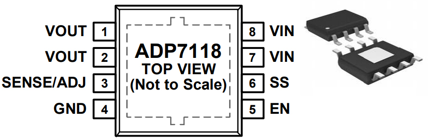
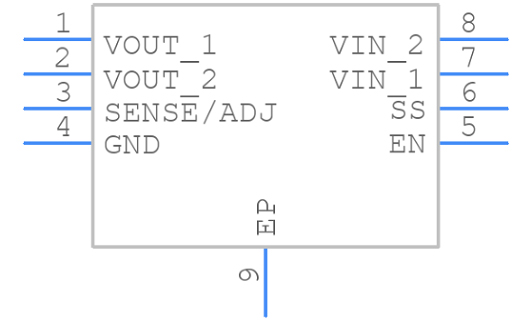
ADP7118 Pinout

ADP7118 CAD Model

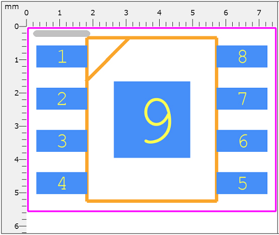
PCB Symbol

PCB Footprint

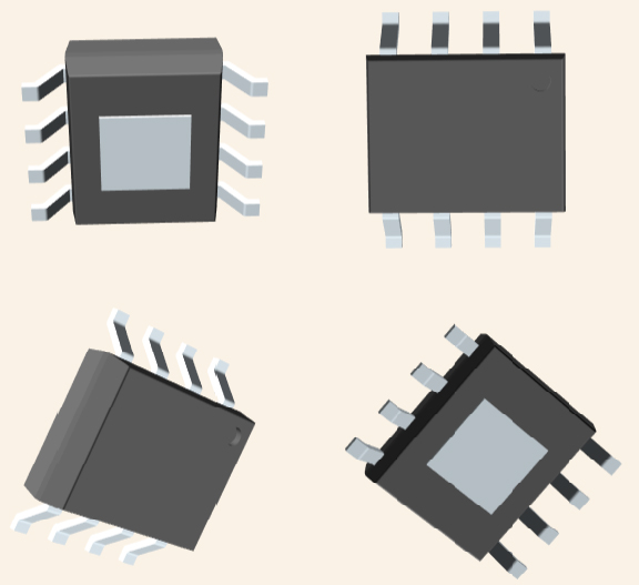
3D Model

ADP7118 Overview

The ADP7118 is a CMOS, low dropout (LDO) linear regulator that operates from 2.7 V to 20 V and provides up to 200 mA of output current. This high input voltage LDO is ideal for the regulation of high performance analog and mixed-signal circuits operating from 20 V down to 1.2 V rails. Using an advanced proprietary architecture, the device provides high power supply rejection, low noise, and achieves excellent line and load transient response with a small 2.2 μF ceramic output capacitor. The ADP7118 regulator output noise is 11 μV rms independent of the output voltage for the fixed options of 5 V or less. The ADP7118 is available in 16 fixed output voltage options. The following voltages are available from stock: 1.2 V (adjustable), 1.8 V, 2.5 V, 3.3 V, 4.5 V, and 5.0 V. Additional voltages available by special order are 1.5 V, 1.85 V, 2.0 V, 2.2 V, 2.75 V, 2.8 V, 2.85 V, 3.8 V, 4.2 V, and 4.6 V.

This article provides you with a basic overview of the ADP7118 Linear Regulator, including its pin descriptions, features and specifications, etc., to help you quickly understand what ADP7118 is.

ADP7118 Features

● Low noise: 11 μV rms independent of fixed output voltage PSRR of 88 dB at 10 kHz, 68 dB at 100 kHz, 50 dB at 1                 MHz, VOUT ≤ 5 V, VIN = 7 V

● Input voltage range: 2.7 V to 20 V

● Maximum output current: 200 mA

● Initial accuracy: ±0.8%

● Accuracy over line, load, and temperature

   ◆ −1.2% to +1.5%, TJ = −40°C to +85°C

   ◆ ±1.8%, TJ = −40°C to +125°C

● Low dropout voltage: 200 mV (typical) at a 200 mA load, VOUT = 5 V

● User programmable soft start (LFCSP and SOIC only)

● Low quiescent current, IGND = 50 μA (typical) with no load

● Low shutdown current: 1.8 μA at VIN = 5 V, 3.0 μA at VIN = 20 V

● Stable with a small 2.2 μF ceramic output capacitor

● Fixed output voltage options: 1.8 V, 2.5 V, 3.3 V, 4.5 V, and 5.0 V, 16 standard voltages between 1.2 V and 5.0 V are                 available

● Adjustable output from 1.2 V to VIN – VDO, output can be adjusted above initial set point

● Precision enable

● 2 mm × 2 mm, 6-lead LFCSP, 8-Lead SOIC, 5-Lead TSOT

● AEC-Q100 qualified for automotive applications

ADP7118 Advantage

The ADP7118 is available in a 6-lead, 2 mm × 2 mm LFCSP making it not only a very compact solution, but it also provides excellent thermal performance for applications requiring up to 200 mA of output current in a small, low profile footprint. The ADP7118 is also available in a 5-lead TSOT and an 8-lead SOIC. The ADP7118 is available in 16 fixed output voltage options, ranging from 1.2 V to 5.0 V. The ADP7118 architecture allows any fixed output voltage to be set to a higher voltage with an external voltage divider.

The ADP7118 uses the EN pin to enable and disable the VOUT pin under normal operating conditions. When EN is high, VOUT turns on, and when EN is low, VOUT turns off. For automatic startup, EN can be tied to VIN. The ADP7118 is supported by the ADIsimPower™ design tool set. ADIsimPower is a collection of tools that produce complete power designs optimized for a specific design goal. The tools enable the user to generate a full schematic, bill of materials, and calculate performance in minutes. The ADP7118 is designed for operation with small, space-saving ceramic capacitors, but functions with general-purpose capacitors as long as care is taken with regard to the effective series resistance (ESR) value. The ADP7118 uses an internal soft start (SS pin open) to limit the inrush current when the output is enabled. The ADP7118 is protected against damage due to excessive power dissipation by current and thermal overload protection circuits. The ADP7118 is designed to current limit when the output load reaches 400 mA (typical). When the output load exceeds 400 mA, the output voltage is reduced to maintain a constant current limit.

Specifications

Analog Devices Inc. ADP7118ARDZ-2.5 technical specifications, attributes, parameters and parts with similar specifications to Analog Devices Inc. ADP7118ARDZ-2.5.

ADP7118ARDZ-2.5 Tech Specifications

Analog Devices Inc. ADP7118ARDZ-2.5 technical specifications, attributes, parameters and parts with similar specifications to Analog Devices Inc. ADP7118ARDZ-2.5.

Product Attribute Attribute Value
Lifecycle StatusPRODUCTION (Last Updated: 1 month ago)
Factory Lead Time8 Weeks
MountSurface Mount
Mounting TypeSurface Mount
Package / Case8-SOIC (0.154, 3.90mm Width) Exposed Pad
Number of Pins8Pins
Operating Temperature-40°C~125°C TA
PackagingTube
JESD-609 Codee3
Pbfree Codeno
Part StatusActive
Moisture Sensitivity Level (MSL)3 (168 Hours)
Number of Terminations8Terminations
ECCN CodeEAR99
Terminal FinishMatte Tin (Sn)
Terminal PositionDUAL
Product Attribute Attribute Value
Terminal FormGULL WING
Peak Reflow Temperature (Cel)260
Number of Functions1Function
Time@Peak Reflow Temperature-Max (s)30
Base Part NumberADP7118
Pin Count8
Current - Supply (Max)320μA
Number of Outputs1Output
Qualification StatusNot Qualified
Voltage - Input (Max)20V
Output Voltage2.5V
Output TypeFixed
Max Output Current200mA
Output ConfigurationPositive
Quiescent Current140μA
Control FeaturesEnable, Soft Start
Product Attribute Attribute Value
Accuracy0.8 %
Output Voltage 12.5V
Number of Regulators1Regulator
Min Input Voltage2.7V
Protection FeaturesOver Current, Over Temperature
Current - Quiescent (Iq)140μA
Voltage Dropout (Max)0.42V @ 200mA
PSRR88dB ~ 50dB (10kHz ~ 1MHz)
Voltage Tolerance-Max2%
Min Current Limit250mA
Input Voltage Absolute-Max44V
Height1.65mm
Length5mm
Width4mm
RoHS StatusROHS3 Compliant
Lead FreeContains Lead
0 Products View Similar

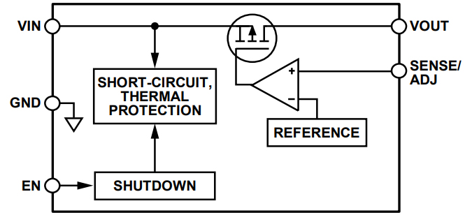
ADP7118 Functional Block Diagram

Internal Block Diagram

ADP7118 Equivalent

                Model number                Manufacturer                                         Description
ADP7118ARDZ-2.5-R7 Analog Devices Inc 20 V, 200 mA, Low Noise, CMOS LDO Linear Regulator
ADP7118AUJZ-2.5-R7 Analog Devices Inc 20 V, 200 mA, Low Noise, CMOS LDO Linear Regulator

ADP7118 Applications

● Regulation to noise sensitive applications

● ADC and DAC circuits, precision amplifiers, power for VCO VTUNE control

● Communications and infrastructure

● Medical and healthcare

● Industrial and instrumentation

● Supported by ADIsimPower tool

ADP7118 Package

8-Lead Standard Small Outline Package

ADP7118 Manufacturer

Analog Devices (NASDAQ: ADI) is a world leader in the design, manufacture, and marketing of a broad portfolio of high performance analog, mixed-signal, and digital signal processing (DSP) integrated circuits (ICs) used in virtually all types of electronic equipment. Since our inception in 1965, we have focused on solving the engineering challenges associated with signal processing in electronic equipment. Used by over 100,000 customers worldwide, our signal processing products play a fundamental role in converting, conditioning, and processing real-world phenomena such as temperature, pressure, sound, light, speed, and motion into electrical signals to be used in a wide array of electronic devices.

Datasheet PDF

ADP7118ARDZ-2.5 Documents

Download datasheets and manufacturer documentation for ADP7118ARDZ-2.5

Frequently Asked Questions

What is the essential property of the ADP7118?
The ADP7118 is a CMOS, low dropout (LDO) linear regulator that operates from 2.7 V to 20 V and provides up to 200 mA of output current.
Does ADP7118 have excessive power protection?
The ADP7118 is protected against damage due to excessive power dissipation by current and thermal overload protection circuits. The ADP7118 is designed to current limit when the output load reaches 400 mA (typical). When the output load exceeds 400 mA, the output voltage is reduced to maintain a constant current limit.
FAQ
What is the essential property of the ADP7118?
The ADP7118 is a CMOS, low dropout (LDO) linear regulator that operates from 2.7 V to 20 V and provides up to 200 mA of output current.
Does ADP7118 have excessive power protection?
The ADP7118 is protected against damage due to excessive power dissipation by current and thermal overload protection circuits. The ADP7118 is designed to current limit when the output load reaches 400 mA (typical). When the output load exceeds 400 mA, the output voltage is reduced to maintain a constant current limit.

TAGS

Share