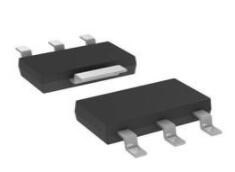
IC REG LIN POS ADJ 800MA SOT223
The TLV1117IDCYG3 device is a positive low-dropout voltage regulator。 This article mainly covers its datasheet, pinout, application, circuit and more about TLV1117IDCYG3.

IC REG LIN POS ADJ 800MA SOT223 The TLV1117IDCYG3 device is a positive low-dropout voltage regulator。 This article mainly covers its datasheet, pinout, application, circuit and more about TLV1117IDCYG3.
57
Mar 3, 2022
Felix Becky
IC REG LIN POS ADJ 800MA SOT223
The TLV1117IDCYG3 device is a positive low-dropout voltage regulator。 This article mainly covers its datasheet, pinout, application, circuit and more about TLV1117IDCYG3.
TLV1117IDCYG3
| Quantity | Unit Price | Ext. Price |
|---|---|---|
| 1+ | $1.08175 | $1.08 |
| 10+ | $1.02052 | $10.21 |
| 100+ | $0.96275 | $96.28 |
| 500+ | $0.90826 | $454.13 |
| 1000+ | $0.85685 | $856.85 |
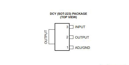
TLV1117IDCYG3 Pinout
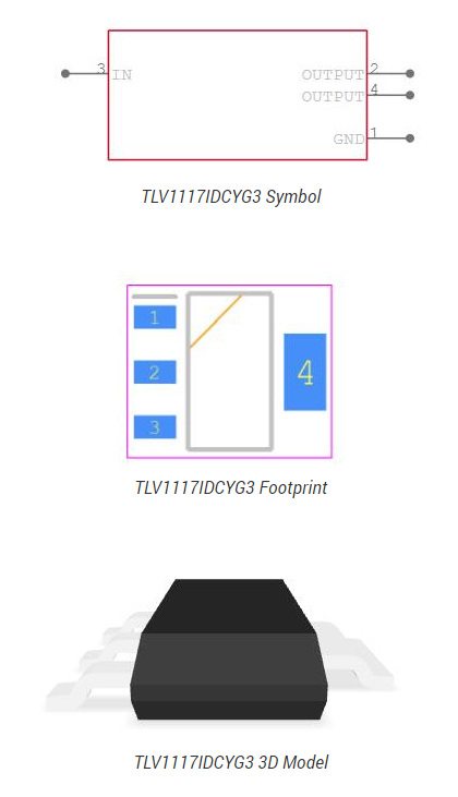
The TLV1117IDCYG3 is a positive low-dropout voltage regulator designed to provide up to 800 mA of output current. The device is available in 1.5-V, 1 .8-V, 2.5-V, 3.3-V, 5-V, and adjustable-output voltage options. All internal circuitry is designed to operate down to a 1-V input-to-output differential. Dropout voltage is specified at a maximum of 1.3 V at 800 mA, decreasing at lower load currents.
1.5-V, 1.8-V, 2.5-V, 3.3-V, 5-V, and Adjustable-Output Voltage Options
Output Current of 800 mA
Specified Dropout Voltage at Multiple Current Levels
0.2% Line Regulation Maximum
0.4% Load Regulation Maximum
Electronic Points of Sale
Medical, Health, and Fitness Applications
Printers
Appliances and White Goods
TV Set-Top Boxes
The adjustable version of the TLV1117 will take a 2.7 to 15-V input. The voltage VREF refers to the voltage between the output and the ADJUST pin, typically 1.25 V. The VREF voltage causes a current to flow across R1, which is the same current that will flow across R2 (minus the negligible 50-µA IADJ). Therefore, R2 can be adjusted to create a larger voltage drop from GND and set the output voltage. The typical application circuit is shown below.
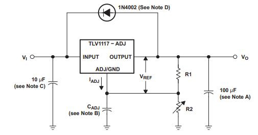
TLV1117IDCYG3-Basic Adjustable Regulator
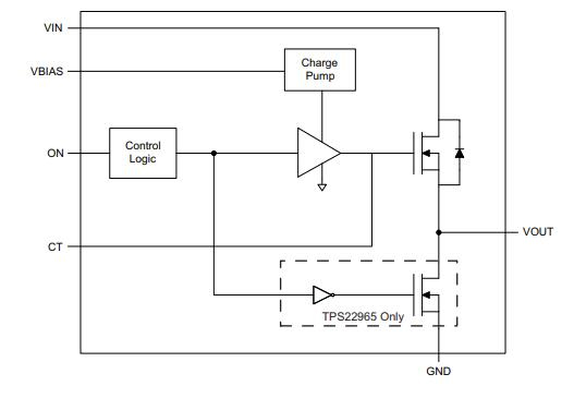
TPS22965 Functional Block Diagram
Texas Instruments TLV1117IDCYG3 technical specifications, attributes, parameters and parts with similar specifications to Texas Instruments TLV1117IDCYG3.
| Product Attribute | Attribute Value | |
|---|---|---|
| Factory Lead Time | 6 Weeks | |
| Mount | Surface Mount | |
| Mounting Type | Surface Mount | |
| Package / Case | TO-261-4, TO-261AA | |
| Number of Pins | 4Pins | |
| Operating Temperature | -40°C~125°C | |
| Packaging | Tube | |
| JESD-609 Code | e3 | |
| Pbfree Code | yes | |
| Part Status | ACTIVE (Last Updated: 4 days ago) | |
| Moisture Sensitivity Level (MSL) | 1 (Unlimited) | |
| Number of Terminations | 4Terminations | |
| ECCN Code | EAR99 | |
| Terminal Finish | Matte Tin (Sn) | |
| Terminal Position | DUAL | |
| Terminal Form | GULL WING | |
| Peak Reflow Temperature (Cel) | 260 |
| Product Attribute | Attribute Value | |
|---|---|---|
| Number of Functions | 1Function | |
| Terminal Pitch | 2.3mm | |
| Base Part Number | TLV1117 | |
| Number of Outputs | 1Output | |
| Voltage - Input (Max) | 15V | |
| Output Type | Adjustable | |
| Current - Output (Max) | 800mA | |
| Output Configuration | Positive | |
| Quiescent Current | 1.7mA | |
| Max Output Voltage | 13.7V | |
| Voltage - Output | 13.75V | |
| Voltage - Output (Min/Fixed) | 1.25V | |
| Number of Regulators | 1Regulator | |
| Min Input Voltage | 2.7V | |
| Protection Features | Over Current, Over Temperature | |
| Voltage Dropout (Max) | 1.3V @ 800mA | |
| PSRR | 75dB (120Hz) |
| Product Attribute | Attribute Value | |
|---|---|---|
| Reference Voltage | 1.262V | |
| Dropout Voltage | 1.2V | |
| Dropout Voltage1-Nom | 1.2V | |
| Min Output Voltage | 1.238V | |
| Min Current Limit | 800mA | |
| Input Bias Current | 5mA | |
| Load Regulation-Max(%) | 0.5% | |
| Height | 1.8mm | |
| Length | 6.5mm | |
| Width | 3.5mm | |
| Thickness | 1.6mm | |
| REACH SVHC | No SVHC | |
| Radiation Hardening | No | |
| RoHS Status | ROHS3 Compliant | |
| Lead Free | Lead Free |
Download datasheets and manufacturer documentation for TLV1117IDCYG3
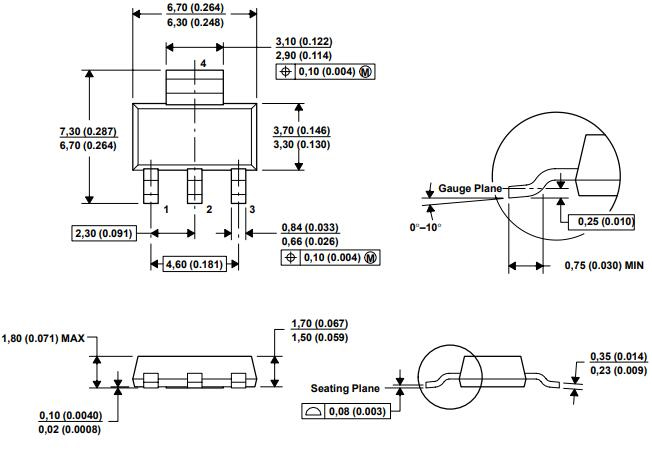
TLV1117IDCYG3 Package
TAGS
Comments