MOSFET - Enhancement Type MOSFET Explained
MOSFET P-CH 30V 11A 8DFN
AON7403 is a 30V P-Channel MOSFET. This article is going to explain guidance details about AON7403 MOSFET and explain the types and usage of p-channel MOSFET.

MOSFET P-CH 30V 11A 8DFN AON7403 is a 30V P-Channel MOSFET. This article is going to explain guidance details about AON7403 MOSFET and explain the types and usage of p-channel MOSFET.
4220
Jan 21, 2022
Nancy Senior
MOSFET - Enhancement Type MOSFET Explained
MOSFET P-CH 30V 11A 8DFN
AON7403 is a 30V P-Channel MOSFET. This article is going to explain guidance details about AON7403 MOSFET and explain the types and usage of p-channel MOSFET.
AON7403
| Quantity | Unit Price | Ext. Price |
|---|---|---|
| 1+ | $0.41788 | $0.42 |
| 10+ | $0.39423 | $3.94 |
| 100+ | $0.37191 | $37.19 |
| 500+ | $0.35086 | $175.43 |
| 1000+ | $0.331 | $331 |
AON7403 is a 30V P-Channel MOSFET. The AON7403 uses advanced trench technology to provide excellent RDS (ON), and ultra-low low gate charge with a 25V gate rating. This device is suitable for use as a load switch or in PWM applications.
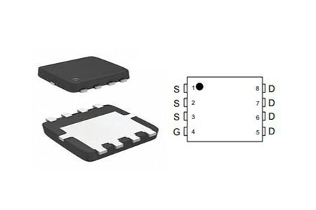
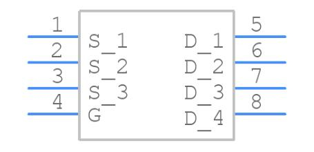
AON7403 Symbol
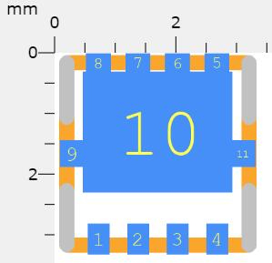
AON7403 Footprint
Alpha & Omega Semiconductor Inc. AON7403 technical specifications, attributes, parameters and parts with similar specifications to Alpha & Omega Semiconductor Inc. AON7403.
Alpha & Omega Semiconductor Inc. AON7403 technical specifications, attributes, parameters and parts with similar specifications to Alpha & Omega Semiconductor Inc. AON7403.
| Product Attribute | Attribute Value | |
|---|---|---|
| Factory Lead Time | 16 Weeks | |
| Mount | Surface Mount | |
| Mounting Type | Surface Mount | |
| Package / Case | 8-PowerVDFN | |
| Number of Pins | 8Pins | |
| Transistor Element Material | SILICON | |
| Current - Continuous Drain (Id) @ 25℃ | 11A Ta 29A Tc | |
| Drive Voltage (Max Rds On, Min Rds On) | 5V 10V | |
| Number of Elements | 1 Element | |
| Power Dissipation (Max) | 3.1W Ta 25W Tc | |
| Voltage - Gate Threshold (Vgs(th)) (Max) @ Id | 3V @ 250μA | |
| Operating Temperature | -55°C~150°C TJ | |
| Packaging | Tape & Reel (TR) |
| Product Attribute | Attribute Value | |
|---|---|---|
| Published | 2011 | |
| Part Status | Obsolete | |
| Moisture Sensitivity Level (MSL) | 1 (Unlimited) | |
| Number of Terminations | 5Terminations | |
| ECCN Code | EAR99 | |
| Terminal Position | DUAL | |
| Terminal Form | FLAT | |
| JESD-30 Code | S-PDSO-F5 | |
| Qualification Status | Not Qualified | |
| Configuration | SINGLE WITH BUILT-IN DIODE | |
| Operating Mode | ENHANCEMENT MODE | |
| Power Dissipation | 25W | |
| Case Connection | DRAIN |
| Product Attribute | Attribute Value | |
|---|---|---|
| FET Type | P-Channel | |
| Transistor Application | SWITCHING | |
| Rds On (Max) @ Id, Vgs | 18m Ω @ 8A, 10V | |
| Input Capacitance (Ciss) (Max) @ Vds | 1400pF @ 15V | |
| Gate Charge (Qg) (Max) @ Vgs | 24nC @ 15V | |
| Drain to Source Voltage (Vdss) | 30V | |
| Vgs (Max) | ±25V | |
| Continuous Drain Current (ID) | 29A | |
| Gate to Source Voltage (Vgs) | 25V | |
| DS Breakdown Voltage-Min | 30V | |
| RoHS Status | ROHS3 Compliant |
Type of Transistor: MOSFET
Type of Control Channel: P -Channel
Maximum Power Dissipation (Pd): 25 W
Maximum Drain-Source Voltage |Vds|: 30 V
Maximum Gate-Source Voltage |Vgs|: 25 V
Maximum Gate-Threshold Voltage |Vgs(th)|: 3 V
Maximum Drain Current |Id|: 29 A
Maximum Junction Temperature (Tj): 150 °C
Rise Time (tr): 8.5 nS
Drain-Source Capacitance (Cd): 240 pF
Maximum Drain-Source On-State Resistance (Rds): 0.018 Ohm
AON7280 , AON7290 , AON7292 , AON7296 , AON7400 , AON7400A , AON7401 , AON7402 , 2N5484 , AON7404 , AON7405 , AON7406 , AON7407 , AON7408 , AON7409 , AON7410 , AON7412
How a P-Channel Enhancement -type MOSFET Works
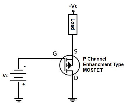
Apply a positive voltage VS to the source of a P-Channel Enhancement -type MOSFET and a negative voltage to the gate terminal of the MOSFET to turn it on (the gate must be sufficiently more negative than the threshold voltage across the drain-source region) (VGDS). A current will be able to pass across the source-drain channel as a result of this.
The P-Channel Enhancement -type MOSFET is completely functional and in the active 'ON' mode of operation when a sufficiently positive voltage, VS, is applied to the source and load, and a sufficient negative voltage is applied to the gate.
To turn off a P-channel enhancement type MOSFET. there are 2 steps you can take. You can either cut off the bias positive voltage, VS, that powers the source. Or you can turn off the negative voltage going to the gate of the transistor.
How a P-Channel Depletion Type MOSFET Works
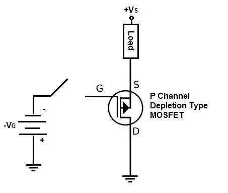
The gate voltage feeding the gate terminal should be 0V to turn on a P-Channel Depletion-Type MOSFET for maximum operation. The drain current is at its maximum magnitude when the gate voltage is 0V, and the transistor is in the active 'ON' zone of conduction.
There are two methods for turning off a P-channel MOSFET, You can either turn off the bias positive voltage, VDD, which drives the drain, or you can leave it on. Alternatively, a negative voltage can be applied to the gate. The current is lowered when a negative voltage is applied to the gate. The current decreases as the gate voltage, VG, grows more negative until cutoff, at which point the MOSFET is in the 'OFF' state. A huge source-drain current is halted.
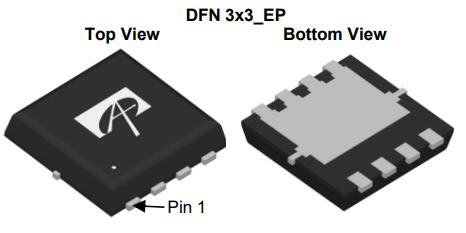
AON7403 Dimensions
Alpha and Omega Semiconductor, Inc., or AOS, is a designer, developer, and global supplier of a broad range of power semiconductors, including a wide portfolio of Power MOSFET and Power IC products. AOS seeks to differentiate itself by integrating its expertise in device physics, process technology, design, and advanced packaging to optimize product performance and cost, and its product portfolio is designed to meet the ever-increasing power efficiency requirements in high volume applications, including portable computers, flat-panel TVs, battery packs, portable media players and power supplies.
Similar Parts from AOS:
ao3401
ao3407a
aod403
ao3413
ao4409
aon7410
Download datasheets and manufacturer documentation for AON7403
TAGS
Comments