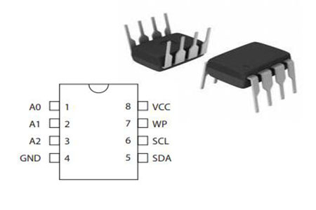
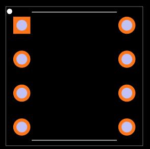
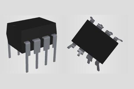
With the help of a little example circuit schematic, let's learn how to use the AT24C256 EEPROM IC. The AT24C256 EEPROM IC communicates with the help of the I2C protocol. The circuit diagram for connecting an EEPROM IC to a microcontroller is given in the diagram below. The IC is given a supply voltage of 3.3 or 5 volts, and its communication lines are linked as indicated in the circuit diagram below.

AT24C256 EEPROM Circuit
Connect pin 6 SCK (Serial Clock) to the microcontroller's SCK pin and pin 5 SDA (Serial Data) to the microcontroller's SDA pin. Two pull-up resistors are used to pull the SCK and SDA pins to a high communication line, similar to I2C communication. This aids in maintaining the bus's idle state at a high level.
When more than one EEPROM or I2C device is connected to the same MCU, the A0, A1, and A2 select pins of this IC are used (Microcontroller unit). These address pins are otherwise connected to the ground. These three pins are linked to the GPIO pins in the preceding circuit layout because more than one EEPROM IC can be cascaded if necessary.
The Write Protect Pin on pin 7 of the AT24C256 EEPROM is utilized to strengthen data security in this IC. If WP (Write Protect) is set to zero (logic 0), the data on the EEPROM IC can be deleted or written. The data written on the IC is otherwise unchanged. If data security isn't a concern, this pin can be grounded (0). Regardless of the state of the WP pin, we can read the data from the EEPROM.
After successful communication, we can program the MCU to write/read the data to the EEPROM IC by using the values of the right register. Firstly we should specify the address of the location to where the data is to be read/written. This shows the normal process of how the data is read/written byte by byte.
An additional option of Page Write is provided by the equivalent 24LC512 EEPROM IC so that the user can write the data of 126 bytes continuously without mentioning any address of each byte of data.
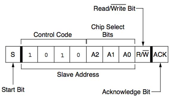
The data interchange between the microcontroller and the EEPROM IC is depicted in the diagram above. The complete message may be broken down into four parts: the start bit, the slave address, the read/write bit, and finally the acknowledgment bit. The Slave address is further broken down into Control code and chip select bits. Because the control code is hardcoded and we are unable to change it, the value will always be 1010. The MCU determines the value of Chip Select bits. For example, if all three pins A2, A1, and A0 are set to low, the device's address will be 0x50. To learn more about how to communicate with the IC, read the datasheet at the bottom of the page.