ATTENTION: Due to increased demand and order volume, processing time may take an additional 1-3 business days.
HomeCommunitySubjectAT45DB081E 8-Mbit DataFlash: Pinout, Features and Datasheet

AT45DB081E 8-Mbit DataFlash: Pinout, Features and Datasheet

NOR Flash Serial-SPI 1.8V/2.5V/3.3V 8M-bit 1M x 8 7ns 8-Pin UDFN EP Tray The AT45DB081E is a 1.7V minimum, serial-interface sequential access Flash memory ideally suited for a wide variety of digital voice, image, program code, and data storage applications.

107

Mar 23, 2022

Vicky Dorothy

DataFlash Overview


NOR Flash Serial-SPI 1.8V/2.5V/3.3V 8M-bit 1M x 8 7ns 8-Pin UDFN EP Tray

The AT45DB081E is a 1.7V minimum, serial-interface sequential access Flash memory ideally suited for a wide variety of digital voice, image, program code, and data storage applications. The AT45DB081E also supports the RapidS serial interface for applications requiring very high speed operation. Furthermore, Huge range of Semiconductors, Capacitors, Resistors and IcS in stock. Welcome RFQ.


AT45DB081E-MHN-Y

5000In Stock
Min.: 1 Mult.: 1
Price not displayed? Not available to buy online? Please send an RFQ, and we will respond immediately.
Quick Links

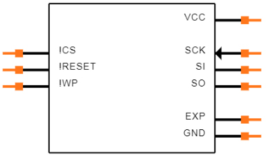
AT45DB081E Pinout

Pinout

AT45DB081E CAD Model

The followings are AT45DB081E Symbol, Footprint, and 3D Model.

Symbol


Footprint


3D Model

AT45DB081E Description

The AT45DB081E is a 1.7V minimum, serial-interface sequential access Flash memory ideally suited for a wide variety of digital voice, image, program code, and data storage applications. The AT45DB081E also supports the RapidS serial interface for applications requiring very high speed operation. Its 8,650,752 bits of memory are organized as 4,096 pages of 256 bytes or 264 bytes each. In addition to the main memory, the AT45DB081E also contains two SRAM buffers of 256/264 bytes each. The buffers allow receiving of data while a page in the main memory is being reprogrammed.

To allow for simple in-system re-programmability, the AT45DB081E does not require high input voltages for programming. The device operates from a single 1.7V to 3.6V power supply for the erase and program and read operations. The AT45DB081E is enabled through the Chip Select pin and accessed via a 3-wire interface consisting of the Serial Input (SI), Serial Output (SO), and the Serial Clock (SCK). All programming and erase cycles are self-timed.

This article provides you with a basic overview of the AT45DB081E 8-Mbit DataFlash, including its pin descriptions, features and specifications, etc., to help you quickly understand what AT45DB081E is.


AT45DB081E Features

● Single 1.7V - 3.6V supply

● Serial Peripheral Interface (SPI) compatible

   ◆ Supports SPI modes 0 and 3

   ◆ Supports RapidS™ operation

● Continuous read capability through entire array

   ◆ Up to 85MHz

   ◆ Low-power read option up to 15MHz

   ◆ Clock-to-output time (tV) of 6ns maximum

● User configurable page size

   ◆ 256 bytes per page

   ◆ 264 bytes per page (default)

   ◆ Page size can be factory pre-configured for 256 bytes

● Two fully independent SRAM data buffers (256/264 bytes)

   ◆ Allows receiving data while reprogramming the main memory array

● Flexible programming options

   ◆ Byte/Page Program (1 to 256/264 bytes) directly into main memory

   ◆ Buffer Write

   ◆ Buffer to Main Memory Page Program

● Flexible erase options

   ◆ Page Erase (256/264 bytes)

   ◆ Block Erase (2KB)

   ◆ Sector Erase (64KB)

   ◆ Chip Erase (8-Mbits)

● Program and Erase Suspend/Resume

● Advanced hardware and software data protection features

   ◆ Individual sector protection

   ◆ Individual sector lockdown to make any sector permanently read-only

● 128-byte, One-Time Programmable (OTP) Security Register

   ◆ 64 bytes factory programmed with a unique identifier

   ◆ 64 bytes user programmable

● Hardware and software controlled reset options

● JEDEC Standard Manufacturer and Device ID Read

● Low-power dissipation

   ◆ 400nA Ultra-Deep Power-Down current (typical)

   ◆ 4.5µA Deep Power-Down current (typical)

   ◆ 25µA Standby current (typical)

   ◆ 11mA Active Read current (typical at 20MHz)

● Endurance: 100,000 program/erase cycles per page minimum

● Data retention: 20 years

● Complies with full industrial temperature range

● Green (Pb/Halide-free/RoHS compliant) packaging options

   ◆ 8-lead SOIC (0.150" wide and 0.208" wide)

   ◆ 8-pad Ultra-thin DFN (5 x 6 x 0.6mm)

   ◆ 8-ball (2 x4 Array) Wafer Level Chip Scale Package

   ◆ Die in Wafer Form

Specifications

AT45DB081E-MHN-Y Tech Specifications

Adesto Technologies AT45DB081E-MHN-Y technical specifications, attributes, parameters and parts with similar specifications to Adesto Technologies AT45DB081E-MHN-Y.

Product Attribute Attribute Value
Factory Lead Time8 Weeks
Contact PlatingGold
MountSurface Mount
Mounting TypeSurface Mount
Package / Case8-UDFN Exposed Pad
Number of Pins8Pins
Weight9.49709mg
Memory TypesNon-Volatile
Operating Temperature-40°C~85°C TC
PackagingTray
Published2012
JESD-609 Codee4
Part StatusActive
Moisture Sensitivity Level (MSL)1 (Unlimited)
Number of Terminations8Terminations
Voltage - Supply1.7V~3.6V
Terminal PositionDUAL
Product Attribute Attribute Value
Peak Reflow Temperature (Cel)260
Number of Functions1Function
Supply Voltage3V
Terminal Pitch1.27mm
Time@Peak Reflow Temperature-Max (s)NOT SPECIFIED
Qualification StatusNot Qualified
Supply Voltage-Max (Vsup)3.6V
Supply Voltage-Min (Vsup)1.7V
InterfaceSPI, Serial
Memory Size8Mb 264Bytes x 4096 pages
Nominal Supply Current15mA
Max Supply Current15mA
Clock Frequency85MHz
Access Time7 ns
Memory FormatFLASH
Memory InterfaceSPI
Data Bus Width8b
Product Attribute Attribute Value
Memory Width1
Write Cycle Time - Word, Page8μs, 4ms
Address Bus Width21b
Density8 Mb
Standby Current-Max0.000001A
Sync/AsyncSynchronous
Word Size8b
Programming Voltage2.7V
Serial Bus TypeSPI
Endurance100000 Write/Erase Cycles
Data Retention Time-Min20
Write ProtectionHARDWARE/SOFTWARE
Length6mm
Height Seated (Max)0.6mm
RoHS StatusROHS3 Compliant
0 Products View Similar

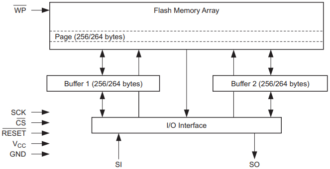
AT45DB081E Functional Block Diagram

The following is the Block Diagram of AT45DB081E.

Block Diagram

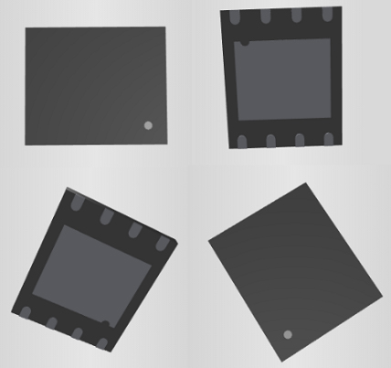
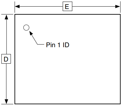
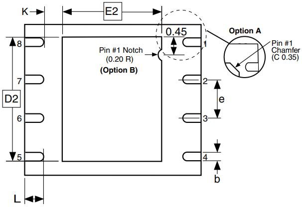
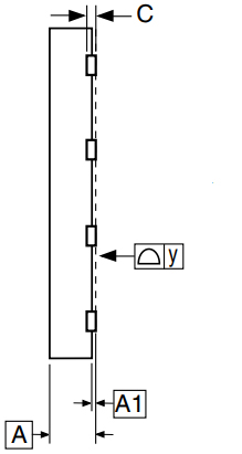
AT45DB081E Package

The following diagrams show the AT45DB081E Package.

Top View


Bottom View


Side View

AT45DB081E Manufacturer

Adesto Technologies provides application-specific and memory solutions optimized for the energy, data and security demands of IoT devices designed for the industrial, consumer, medical and communications markets. Adesto's Flagship memory family: DataFlash: Saves system energy, reduces board part count, saves microcontroller I/Os, widest operating voltage and power fail protection. Fusion: Designed for battery operated devices in the IoT space. Widest operating voltage and lowest standby current in the industry. Standard Flash: Lowest cost alternative, industry standard footprint and densities up to 128 Mb. Moneta: Industry's lowest power memory. Core voltage at 1.2 volts and 50 times lower power than competing data storage solutions.


Datasheet PDF

AT45DB081E-MHN-Y Documents

Download datasheets and manufacturer documentation for AT45DB081E-MHN-Y

Frequently Asked Questions

How many pins of AT45DB081E-MHN-Y?
8 Pins.
What’s the operating temperature of AT45DB081E-MHN-Y?
-40°C~85°C TC.
What is the essential property of the AT45DB081E?
The AT45DB081E is a 1.7V minimum, serial-interface sequential access Flash memory ideally suited for a wide variety of digital voice, image, program code, and data storage applications.
FAQ
How many pins of AT45DB081E-MHN-Y?
8 Pins.
What’s the operating temperature of AT45DB081E-MHN-Y?
-40°C~85°C TC.
What is the essential property of the AT45DB081E?
The AT45DB081E is a 1.7V minimum, serial-interface sequential access Flash memory ideally suited for a wide variety of digital voice, image, program code, and data storage applications.

TAGS

Share