ATTENTION: Due to increased demand and order volume, processing time may take an additional 1-3 business days.
HomeCommunitySubjectATMEGA168 Microcontrollers: Features, Pinout, and Datasheet

ATMEGA168 Microcontrollers: Features, Pinout, and Datasheet

Embedded - Microcontrollers A/D 8x10b 32-TQFP 16kB Brown-out Detect/Reset, POR, PWM, WDT -40°C~85°C TA 1.8V~5.5V AVR? ATmega MICROCONTROLLER, RISC ATMEGA168A 20MHz MCU 8-bit ATmega AVR RISC 16KB Flash 2.5V/3.3V/5V 32-Pin TQFP

262

Nov 2, 2021

Dick Burns

Which one buy? Arduino ATmega328 vs ATmega168. because..

Embedded - Microcontrollers A/D 8x10b 32-TQFP 16kB Brown-out Detect/Reset, POR, PWM, WDT -40°C~85°C TA 1.8V~5.5V AVR® ATmega MICROCONTROLLER, RISC ATMEGA168A 20MHz MCU 8-bit ATmega AVR RISC 16KB Flash 2.5V/3.3V/5V 32-Pin TQFP

The ATMEGA168 is a CMOS 8-bit microcontroller with low power consumption based on the AVR® enhanced RISC architecture that is available in three packages: PDIP, MLF, and TQFP. This article mainly introduces features, pinout, datasheet and other detailed information about Microchip Technology ATMEGA168.

ATMEGA168A-AU

8500In Stock
Min.: 1 Mult.: 1
Quantity Unit Price Ext. Price
1+ $8.11754$8.12
10+ $7.65806$76.58
100+ $7.22458$722.46
500+ $6.81565$3407.83
1000+ $6.42985$6429.85
Unit Price:$8.11754
Subtotal: $8.12
Looking for a better price? Want a lower wholesale price? Please send an RFQ, and we will respond immediately.
Quick Links

ATMEGA168 Pinout

Pinout

ATMEGA168 CAD Model

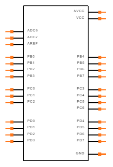
Symbol

Footprint

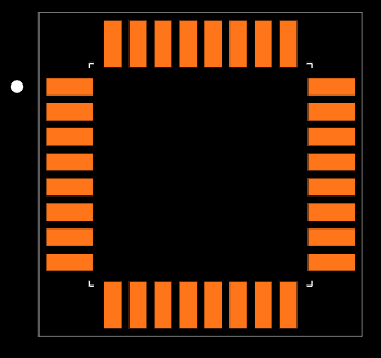
Footprint

ATMEGA168 Features

• High Performance, Low Power AVR® 8-Bit Microcontroller Family

• Advanced RISC Architecture

̶ 131 Powerful Instructions – Most Single Clock Cycle Execution

̶ 32 x 8 General Purpose Working Registers

̶ Fully Static Operation

̶ Up to 20 MIPS Throughput at 20MHz

̶ On-chip 2-cycle Multiplier

• High Endurance Non-volatile Memory Segments

̶ 4/8/16/32KBytes of In-System Self-Programmable Flash program memory

̶ 256/512/512/1KBytes EEPROM

̶ 512/1K/1K/2KBytes Internal SRAM

̶ Write/Erase Cycles: 10,000 Flash/100,000 EEPROM

̶ Data retention: 20 years at 85°C/100 years at 25°C(1)

̶ Optional Boot Code Section with Independent Lock Bits

  In-System Programming by On-chip Boot Program

  True Read-While-Write Operation

̶ Programming Lock for Software Security

• QTouch® library support

̶ Capacitive touch buttons, sliders and wheels

̶ QTouch and QMatrix™ acquisition

̶ Up to 64 sense channels

• Peripheral Features

̶ Two 8-bit Timer/Counters with Separate Prescaler and Compare Mode

̶ One 16-bit Timer/Counter with Separate Prescaler, Compare Mode, and Capture Mode

̶ Real Time Counter with Separate Oscillator

̶ Six PWM Channels

̶ 8-channel 10-bit ADC in TQFP and QFN/MLF package

  Temperature Measurement

̶ 6-channel 10-bit ADC in PDIP Package

  Temperature Measurement

̶ Programmable Serial USART

̶ Master/Slave SPI Serial Interface

̶ Byte-oriented 2-wire Serial Interface (Philips I2C compatible)

̶ Programmable Watchdog Timer with Separate On-chip Oscillator

̶ On-chip Analog Comparator

̶ Interrupt and Wake-up on Pin Change

• Special Microcontroller Features

̶ Power-on Reset and Programmable Brown-out Detection

̶ Internal Calibrated Oscillator

̶ External and Internal Interrupt Sources

̶ Six Sleep Modes: Idle, ADC Noise Reduction, Power-save, Power-down, Standby, and Extended Standby

• I/O and Packages

̶ 23 Programmable I/O Lines

̶ 28-pin PDIP, 32-lead TQFP, 28-pad QFN/MLF and 32-pad QFN/MLF

• Operating Voltage:

̶ 1.8 - 5.5V

• Temperature Range:

̶ -40°C to 85°C

• Speed Grade:

̶ 0 - 4MHz@1.8 - 5.5V, 0 - 10MHz@2.7 - 5.5.V, 0 - 20MHz @ 4.5 - 5.5V

• Power Consumption at 1MHz, 1.8V, 25°C

̶ Active Mode: 0.2mA

̶ Power-down Mode: 0.1µA

  Power-save Mode: 0.75µA (Including 32kHz RTC)

Specifications

ATMEGA168A-AU Tech Specifications

Microchip Technology ATMEGA168A-AU technical specifications, attributes, parameters and parts with similar specifications to Microchip Technology ATMEGA168A-AU.

Product Attribute Attribute Value
Factory Lead Time8 Weeks
Contact PlatingTin
MountSurface Mount
Mounting TypeSurface Mount
Package / Case32-TQFP
Number of Pins32Pins
Data ConvertersA/D 8x10b
Number of I/Os23I/Os
Watchdog TimersYes
Operating Temperature-40°C~85°C TA
PackagingTray
SeriesAVR® ATmega
Published1997
JESD-609 Codee3
Pbfree Codeyes
Part StatusActive
Moisture Sensitivity Level (MSL)3 (168 Hours)
Number of Terminations32Terminations
Terminal PositionQUAD
Terminal FormGULL WING
Peak Reflow Temperature (Cel)260
Product Attribute Attribute Value
Supply Voltage5V
Frequency20MHz
Time@Peak Reflow Temperature-Max (s)40
Base Part NumberATMEGA168A
Supply Voltage-Max (Vsup)5.5V
Power Supplies2/5V
Supply Voltage-Min (Vsup)4.5V
Interface2-Wire, I2C, SPI, Serial, UART, USART
Memory Size16kB
Oscillator TypeInternal
RAM Size1K x 8
Voltage - Supply (Vcc/Vdd)1.8V~5.5V
uPs/uCs/Peripheral ICs TypeMICROCONTROLLER, RISC
Core ProcessorAVR
PeripheralsBrown-out Detect/Reset, POR, PWM, WDT
Program Memory TypeFLASH
Core Size8-Bit
Program Memory Size16KB 8K x 16
ConnectivityI2C, SPI, UART/USART
Bit Size8
Has ADCYES
Product Attribute Attribute Value
DMA ChannelsNO
Data Bus Width8b
Number of Timers/Counters3Timers/Counters
EEPROM Size512 x 8
Boundary ScanNO
Low Power ModeNO
FormatFIXED-POINT
Integrated CacheNO
Number of ADC Channels8ADC Channels
Number of Serial I/Os1Serial I/O
Number of External Interrupts2External Interrupts
Number of PWM Channels6PWM Channels
Number of I2C Channels1I2C Channel
Height1.05mm
Length7mm
Width7mm
REACH SVHCNo SVHC
Radiation HardeningNo
RoHS StatusROHS3 Compliant
Lead FreeLead Free
0 Products View Similar

ATMEGA168 Functional Block Diagram

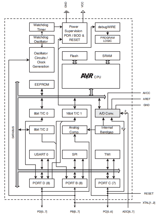
Functional Block Diagram


The AVR core has 32 general-purpose working registers and a large instruction set. The Arithmetic Logic Unit (ALU) is directly coupled to all 32 registers, allowing two independent registers to be accessed in a single instruction executed in one clock cycle. The resulting architecture is more code efficient than traditional CISC microcontrollers, with throughputs up to ten times faster.

The ATMEGA168 has the following capabilities: 4K/8Kbytes of Read-While-Write In-System Programmable Flash, 256/512/512/1Kbytes EEPROM, 512/1K/1K/2Kbytes SRAM, 23 general-purpose I/O lines, 32 general purpose working registers, three flexible Timer/Counters with compare modes, internal and external interrupts, a serial programmable USART, a byte-oriented 2-wire Serial Interface, an SPI serial port, a 6-channel 10-bit ADC The CPU is turned off in Idle mode, while the SRAM, Timer/Counters, USART, 2-wire Serial Interface, SPI interface, and interrupt system remain operational. The Oscillator is frozen in the Power-down mode, which disables all other chip functions until the next interrupt or hardware reset. The asynchronous timer continues to run in Power-save mode, allowing the user to keep a timer base while the rest of the device sleeps. To reduce switching noise during ADC conversions, the ADC Noise Reduction mode turns off the CPU and all I/O modules except the asynchronous timer and ADC. The crystal/resonator Oscillator runs in Standby mode while the rest of the device sleeps. This enables for a very quick start-up while also consuming extremely little power.

While the Application Flash part is being updated, the software in the Boot Flash area will continue to operate, allowing for genuine Read-While-Write operation. The ATMEGA168 is a sophisticated microcontroller that combines an 8-bit RISC CPU with In-System Self-Programmable Flash on a monolithic device to provide a highly versatile and cost effective solution to many embedded control applications.

C Compilers, Macro Assemblers, Program Debuggers/Simulators, In-Circuit Emulators, and Evaluation Kits are all available for the ATMEGA168 AVR.

ATMEGA168 Alternative

Part Number Description Manufacturer
ATMEGA168-24AIMICROCONTROLLERS AND PROCESSORS RISC Microcontroller, 8-Bit, FLASH, 24MHz, CMOS, PQFP32, 7 X 7 MM, 1 MM HEIGHT, 0.80 MM PITCH, PLASTIC, MS-026ABA, TQFP-32 Atmel Corporation

ATMEGA168 Applications

• Students Projects

• Embedded and Robotics System

• Industrial Automation

• Home Security System

• For the Designing of Quadcopters

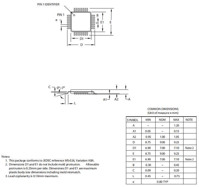
ATMEGA168 Package

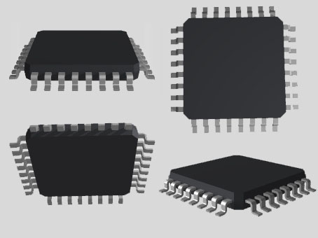
Package

ATMEGA168 Manufacturer

Microchip Technology Inc., a leader in microcontroller and analog semiconductors, is a market leader. The headquarters of Microchip were in Chandler, Arizona. We strive to provide low-risk product development while lowering total system costs and shortening time to market. We primarily service consumers in a variety of fields all across the world. Our mission is to provide outstanding technical support as well as consistent delivery and quality.

Datasheet PDF

ATMEGA168A-AU Documents

Download datasheets and manufacturer documentation for ATMEGA168A-AU

Frequently Asked Questions

1.What tools are needed for ATMEGA168 development?
(1) ATMEGA168 has a complete set of programming and system development tools, including C language compiler, macro assembly, program debugger/software simulator, simulator and evaluation board. (2) ATMEGA168 has the following features: 16K bytes of in-system programmable Flash (with simultaneous read and write capability, namely RWW), 512 bytes of EEPROM, 1K bytes of SRAM, 23 general-purpose I/O lines, 32 general-purpose Working register, DebuyWIRE interface for boundary scan, support for on-chip debugging and programming, three flexible timers/counters (T/C) with comparison mode, on-chip/outside interrupts, programmable serial USART, available The universal serial interface of the initial condition detector, 8-channel 10-bit ADC with optional differential input stage programmable gain (TQFP package), programmable watchdog timer with an on-chip oscillator, an SPI serial port, And five power-saving modes that can be selected through software.
2.The single-chip microcomputer main control chip ATMEGA8/ATNEGA48/ATMEGA88/ATMEGA168 which is better?
ATmega48, ATmega88 and ATmega168 only differ in memory size, boot loader support and interrupt vector length. ATmega88 and ATmega168 support true simultaneous read and write self-programming operations. The chip has an independent BootLoader area, and SPM instructions can only be executed in this FLASH area. However, ATmega48 does not support simultaneous read and write operations. It does not have a separate Boot Loader area. SPM commands can access the entire Flash area. The main difference between ATmega8 and the other three is the lack of external interrupt function and the difference in storage size. The pins of these 4 chips are exactly the same, as long as the packages are the same, they can be upgraded perfectly.
3.What chip is ATMEGA168V-10PU?
Single-chip microcomputer, memory chip.
FAQ
1.What tools are needed for ATMEGA168 development?
(1) ATMEGA168 has a complete set of programming and system development tools, including C language compiler, macro assembly, program debugger/software simulator, simulator and evaluation board. (2) ATMEGA168 has the following features: 16K bytes of in-system programmable Flash (with simultaneous read and write capability, namely RWW), 512 bytes of EEPROM, 1K bytes of SRAM, 23 general-purpose I/O lines, 32 general-purpose Working register, DebuyWIRE interface for boundary scan, support for on-chip debugging and programming, three flexible timers/counters (T/C) with comparison mode, on-chip/outside interrupts, programmable serial USART, available The universal serial interface of the initial condition detector, 8-channel 10-bit ADC with optional differential input stage programmable gain (TQFP package), programmable watchdog timer with an on-chip oscillator, an SPI serial port, And five power-saving modes that can be selected through software.
2.The single-chip microcomputer main control chip ATMEGA8/ATNEGA48/ATMEGA88/ATMEGA168 which is better?
ATmega48, ATmega88 and ATmega168 only differ in memory size, boot loader support and interrupt vector length. ATmega88 and ATmega168 support true simultaneous read and write self-programming operations. The chip has an independent BootLoader area, and SPM instructions can only be executed in this FLASH area. However, ATmega48 does not support simultaneous read and write operations. It does not have a separate Boot Loader area. SPM commands can access the entire Flash area. The main difference between ATmega8 and the other three is the lack of external interrupt function and the difference in storage size. The pins of these 4 chips are exactly the same, as long as the packages are the same, they can be upgraded perfectly.
3.What chip is ATMEGA168V-10PU?
Single-chip microcomputer, memory chip.

TAGS

Share