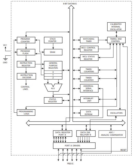
- 120 Powerful Instructions - Most Single Clock Cycle Execution
- 32 x 8 General Purpose Working Registers
- Fully Static Operation
- 2/4/8K Byte of In-System Programmable Program Memory Flash (ATtiny25/45/85)
- 128/256/512 Bytes In-System Programmable EEPROM (ATtiny25/45/85)
- 128/256/512 Bytes Internal SRAM (ATtiny25/45/85)
- Programming Lock for Self-Programming Flash Program and EEPROM Data Security
- 8-bit Timer /Counter with Prescaler and Two PWM Channels
- 8-bit High-Speed Timer /Counter with Separate Prescaler
- USI - Universal Serial Interface with Start Condition Detector
- 10-bit ADC
- Programmable Watchdog Timer with Separate On-chip Oscillator
- On-chip Analog Comparator
- debugWIRE On-chip Debug System
- In-System Programmable via SPI Port
- External and Internal Interrupt Sources
- Low Power Idle, ADC Noise Reduction, and Power-down Modes
- Enhanced Power-on Reset Circuit
- Programmable Brown-out Detection Circuit
- Internal Calibrated Oscillator
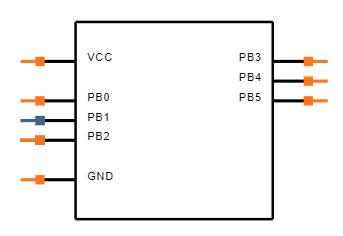
- Six Programmable I/O Lines
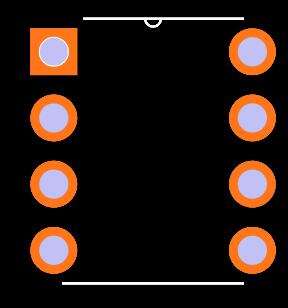
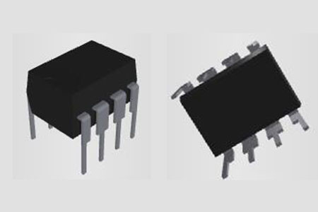
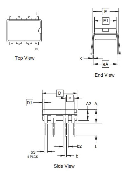
- 8-pin PDIP, 8-pin SOIC and 20-pad QFN/MLF
- 1.8 - 5.5V for ATtiny25 /45/85V
- 2.7 - 5.5V for ATtiny25 /45/85
- ATtiny25 /45/85V: 0 - 4 MHz @ 1.8 - 5.5V, 0 - 10 MHz @ 2.7 - 5.5V
- ATtiny25 /45/85: 0 - 10 MHz @ 2.7 - 5.5V, 0 - 20 MHz @ 4.5 - 5.5V
- Active Mode: 1 MHz, 1.8V: 300 μA
- Power-down Mode: 0.1μA at 1.8V