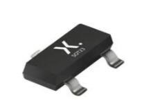
Transistors - FETs, MOSFETs - Single MOSFET N-CH 30V 0.85A SOT23
BSH103 is an N-channel enhancement mode MOS transistor in a SOT23 SMD package. This post will unlock its datasheet, Pinout, application and more details about BSH103.

Transistors - FETs, MOSFETs - Single MOSFET N-CH 30V 0.85A SOT23 BSH103 is an N-channel enhancement mode MOS transistor in a SOT23 SMD package.
142
Dec 11, 2021
Jason Carl
Transistors - FETs, MOSFETs - Single MOSFET N-CH 30V 0.85A SOT23
BSH103 is an N-channel enhancement mode MOS transistor in a SOT23 SMD package. This post will unlock its datasheet, Pinout, application and more details about BSH103.
BSH103,235
| Quantity | Unit Price | Ext. Price |
|---|---|---|
| 1+ | $0.18466 | $0.18 |
| 10+ | $0.17421 | $1.74 |
| 100+ | $0.16435 | $16.43 |
| 500+ | $0.15504 | $77.52 |
| 1000+ | $0.14627 | $146.27 |
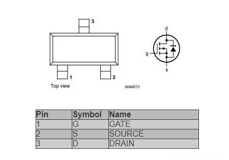
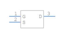
BSH103 Symbol
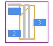
BSH103 Footprint
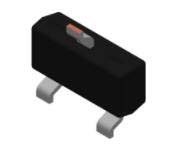
BSH103 3D Model
NXP's BSH103 is a TrenchMOS -based surface mount N channel enhancement mode MOS transistor in the SOT-23 package. This transistor has an extremely low threshold, high switching speed, no secondary breakdown, and a direct CMOS, TTL interface. BSH103 is intended for use in high-frequency applications, as a glue logic bridge between logic blocks or peripherals, in computing, and in battery-powered applications.
Suitable for use with all 5V logic families
Suitable for very low gate drive sources
Drain to source voltage (Vds) of 30V
Gate to source voltage of ±8V
Drain current (Id) of 850mA
Power dissipation (Pd) of 750mW
Operating junction temperature range from -55 °C to 150 °C
Power Management
Consumer Electronics
Portable Devices
Industrial
The alternative for BSH103:
BSH103,235
BSH103,215
The following circuit shows the BSH103 test circuit:
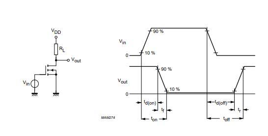
BSH103 Test Circuit
Nexperia USA Inc. BSH103,235 technical specifications, attributes, parameters and parts with similar specifications to Nexperia USA Inc. BSH103,235.
Nexperia USA Inc. BSH103,235 technical specifications, attributes, parameters and parts with similar specifications to Nexperia USA Inc. BSH103,235.
| Product Attribute | Attribute Value | |
|---|---|---|
| Factory Lead Time | 4 Weeks | |
| Contact Plating | Tin | |
| Mounting Type | Surface Mount | |
| Package / Case | TO-236-3, SC-59, SOT-23-3 | |
| Surface Mount | YES | |
| Number of Pins | 3Pins | |
| Transistor Element Material | SILICON | |
| Current - Continuous Drain (Id) @ 25℃ | 850mA Ta | |
| Drive Voltage (Max Rds On, Min Rds On) | 2.5V | |
| Number of Elements | 1 Element | |
| Power Dissipation (Max) | 540mW Ta | |
| Turn Off Delay Time | 20 ns | |
| Voltage - Gate Threshold (Vgs(th)) (Max) @ Id | 400mV @ 1mA (Min) | |
| Operating Temperature | -55°C~150°C TJ | |
| Packaging | Tape & Reel (TR) | |
| Published | 1998 |
| Product Attribute | Attribute Value | |
|---|---|---|
| JESD-609 Code | e3 | |
| Part Status | Active | |
| Moisture Sensitivity Level (MSL) | 1 (Unlimited) | |
| Number of Terminations | 3Terminations | |
| ECCN Code | EAR99 | |
| HTS Code | 8541.21.00.75 | |
| Terminal Position | DUAL | |
| Terminal Form | GULL WING | |
| Peak Reflow Temperature (Cel) | 260 | |
| Time@Peak Reflow Temperature-Max (s) | 30 | |
| Element Configuration | Single | |
| Operating Mode | ENHANCEMENT MODE | |
| Power Dissipation | 500mW | |
| Turn On Delay Time | 2.5 ns | |
| FET Type | N-Channel | |
| Transistor Application | SWITCHING |
| Product Attribute | Attribute Value | |
|---|---|---|
| Rds On (Max) @ Id, Vgs | 400m Ω @ 500mA, 4.5V | |
| Input Capacitance (Ciss) (Max) @ Vds | 83pF @ 24V | |
| Gate Charge (Qg) (Max) @ Vgs | 2.1nC @ 4.5V | |
| Rise Time | 3.5ns | |
| Vgs (Max) | ±8V | |
| Fall Time (Typ) | 3.5 ns | |
| Continuous Drain Current (ID) | 850mA | |
| Gate to Source Voltage (Vgs) | 8V | |
| Max Dual Supply Voltage | 30V | |
| Drain Current-Max (Abs) (ID) | 0.85A | |
| Drain-source On Resistance-Max | 0.5Ohm | |
| Drain to Source Breakdown Voltage | 30V | |
| Radiation Hardening | No | |
| RoHS Status | ROHS3 Compliant |
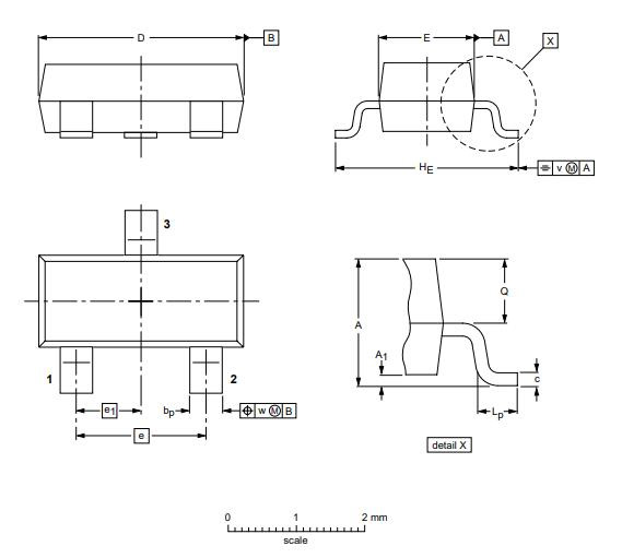
Nexperia is a dedicated global leader in Discretes, Logic and MOSFETs devices. This new company became independent at the beginning of 2017. Focused on efficiency, Nexperia produces consistently reliable semiconductor components at a high volume: 85 billion annually. The company’s extensive portfolio meets the stringent standards set by the Automotive industry. And industry-leading small packages, produced in their own manufacturing facilities, combine power and thermal efficiency with best-in-class quality levels. Built on over half a century of expertise, Nexperia has 11,000 employees across Asia, Europe and the U.S. supporting customers globally.
Download datasheets and manufacturer documentation for BSH103,235
TAGS
Comments