ATTENTION: Due to increased demand and order volume, processing time may take an additional 1-3 business days.
HomeCommunitySubjectCA3140E Operational Amplifier: Diagram, Pinout, and Datasheet

CA3140E Operational Amplifier: Diagram, Pinout, and Datasheet

IC OPAMP GP 4.5MHZ 8DIP The CA3140E is a single monolithic chip that combines the advantages of high voltage PMOS and high voltage bipolar transistors in a single integrated circuit operational amplifier.

688

Jan 19, 2022

Eli Grey

How to Make Efficient Automatic Street Light System using IC CA3140 (Op Amp)


IC OPAMP GP 4.5MHZ 8DIP

The CA3140E is a single monolithic chip that combines the advantages of high voltage PMOS and high voltage bipolar transistors in a single integrated circuit operational amplifier. This article mainly introduces diagram, pinout, datasheet and other detailed information about Intersil (Renesas Electronics America) CA3140E.

CA3140E

35In Stock
Min.: 1 Mult.: 1
Price not displayed? Not available to buy online? Please send an RFQ, and we will respond immediately.
Quick Links

CA3140 Description

The CA3140 is integrated circuit operation amplifier combining the advantages of high voltage PMOS transistor with high voltage bipolar transistor single chip. CA3140 BiMOS operational amplifier MOSFET (PMOS) transistor with gate protection The input circuit provides very high input impedance, very low Input current and high-speed performance. CA3140 operates with a supply voltage of 4V to 36V (single power supply or dual power supply). These op amps Internal phase compensation for stability The unity gain follows the operation in operation, in addition, access terminal with auxiliary external capacitor If additional frequency roll-off is required. terminal too provided for applications that require input offset voltage Zero. The use of PMOS field effect tube at the input end phase causes the common mode input voltage capability to drop 0.5V below the negative power supply terminal, an important

The properties of a single power supply application. Output stage uses bipolar transistors and includes built-in protection prevent damage caused by short-circuit of load terminals to either end power rail or ground. CA3140 for power supply operation The voltage is up to 36V (±18V).

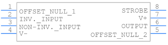
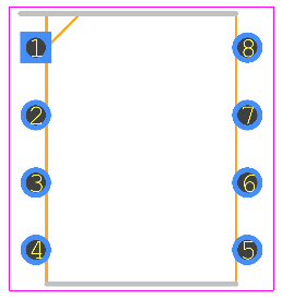
CA3140 Pinout

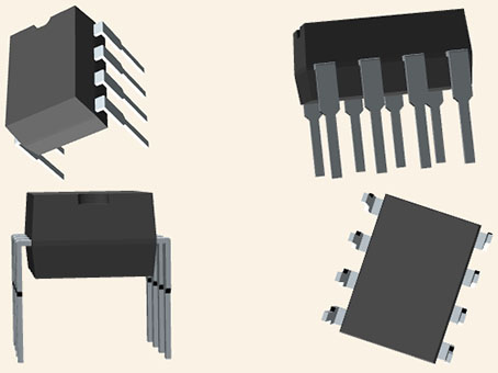
CA3140 CAD Model

Symbol


Footprint


3D Model

CA3140 Features

• MOSFET input stage

-Very high input impedance (ZIN) -1.5TΩ (typical value)

-Very low input current (Il) -10pA (typical value), ±15V

-Wide common mode input voltage range (VlCR)-Can be swung 0.5V below the negative supply voltage rail

-Output swing supplements input common mode range

• Replace the industry type 741 directly in most applications

• Pb-free plus anneal available (compliant with RoHS)

Specifications

Intersil (Renesas Electronics America) CA3140E technical specifications, attributes, parameters and parts with similar specifications to Intersil (Renesas Electronics America) CA3140E.
CA3140E Tech Specifications

Intersil (Renesas Electronics America) CA3140E technical specifications, attributes, parameters and parts with similar specifications to Intersil (Renesas Electronics America) CA3140E.
Product Attribute Attribute Value
Contact PlatingLead, Tin
MountThrough Hole
Package / CaseDIP
Number of Pins8Pins
Published1998
JESD-609 Codee0
Pbfree Codeno
ECCN CodeEAR99
Terminal FinishTin/Lead (Sn/Pb)
Max Operating Temperature125°C
Min Operating Temperature-55°C
Terminal PositionDUAL
Peak Reflow Temperature (Cel)NOT SPECIFIED
Number of Functions1Function
Supply Voltage15V
Terminal Pitch2.54mm
Time@Peak Reflow Temperature-Max (s)NOT SPECIFIED
Product Attribute Attribute Value
Pin Count8
Qualification StatusNot Qualified
Operating Supply Voltage9V
Temperature GradeMILITARY
Max Supply Voltage36V
Min Supply Voltage4V
Operating Supply Current4mA
Supply Current-Max6mA
Slew Rate9 V/μs
ArchitectureVOLTAGE-FEEDBACK
Amplifier TypeOPERATIONAL AMPLIFIER
Common Mode Rejection Ratio90 dB
Current - Input Bias10pA
Output Current per Channel40mA
Input Offset Voltage (Vos)5mV
Gain Bandwidth Product3.7MHz
Neg Supply Voltage-Nom (Vsup)-15V
Product Attribute Attribute Value
Unity Gain BW-Nom4500 kHz
Voltage Gain100dB
Low-OffsetNO
Frequency CompensationYES
Max Dual Supply Voltage18V
Low-BiasYES
Min Dual Supply Voltage2V
Bias Current-Max (IIB) @25C0.00005μA
Dual Supply Voltage9V
Number of Amplifiers1Amplifier
Height4.95mm
Length10.16mm
Width7.11mm
REACH SVHCNo SVHC
RoHS StatusRoHS Compliant
0 Products View Similar

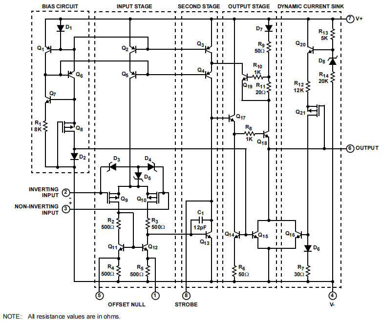
CA3140 Schematic Diagram

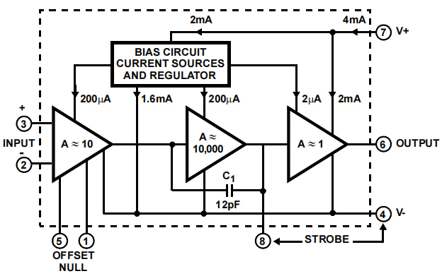
CA3140 Block Diagram

CA3140 Working Principle

In this circuit, low current provides potential as input power, load resistance RL. When the load current is monitored by the power meter M, the load current increases by the multiplication factor R2/R1. Value, if the load current is 100nA, the supply load current 100μA will be submitted, and simpler current measurement uses many low-cost meters.


Remember that the input and output voltage are transferred at the same potential and the output current is amplified by the scale factor. The dotted line component decoupling capacitor FTO prevents potenTIoal oscillations in high output load capacitors. The problem is that the required high-frequency feedback is provided by capacitors to provide load decoupling and dotted series resistors.

Where to use CA3140?

CA3140 is a single package Op-Amp that has been widely used by engineers and students for quite a long time now. This Op-Amp can be used for many general purpose applications like voltage follower, buffers, comparators, amplifiers, adders and much more. So if you looking for a plain old Op-Amp just for some basic circuit design then this IC might be the right choice for you.

How to use CA3140?

CA3140 is very similar to the CA3240 Op Amp. The main difference is that CA3240 has two Op-Amps inside package making to more cost-effective and compact.


One notable unique feature of the CA3140 Op-Amp is that it has two Offset Null pins (pin1 and pin 5). These two pins can be used to correct the offset error of an Op-Amp. That is when the voltage difference between the inverting and no-inverting pins is zero the output voltage of the Op-Amp should also be zero. If not then it is considered as offset error and it can be brought to zero again by providing an offset voltage through the offset pins that would nullify the error.


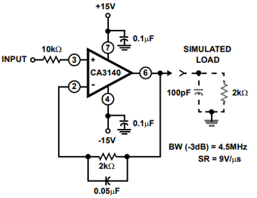
A test circuit of the CA3140 is given below.


CA3140 Applications

• Single-supply amplifier with reference to ground in automotive and portable meters

• Sample and hold amplifier

• Long time timer/multivibrator (Microsecond-minute-hour)

• Photocurrent meter

• Peak detector

• Active filter

• Comparators

• Interfaces in 5V TTL systems and other low supply voltage system

• All standard operational amplifier applications

• Function generator

• Tone control

• power supply

• Portable instrument

• Intrusion alarm system


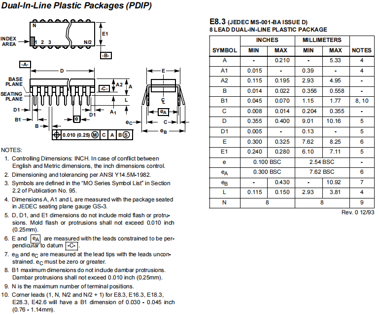
CA3140 Package

CA3140 Manufacturer

Intersil is an American semiconductor company headquartered in Milpitas, California. As of February 24, 2017, Intersil is a subsidiary of Renesas. The predecessor Intersil was established in August 1999 through the acquisition of the semiconductor business of Harris Corporation. Intersil is a power management IC business, with expertise in power management and precision simulation technology applicable to industrial, infrastructure, mobile, automotive and aerospace applications.


Datasheet PDF

Download datasheets and manufacturer documentation for Intersil (Renesas Electronics America) CA3140E.
CA3140E Documents

Download datasheets and manufacturer documentation for CA3140E

Frequently Asked Questions

TAGS

Share