ATTENTION: Due to increased demand and order volume, processing time may take an additional 1-3 business days.
HomeCommunitySubjectCC1101 Transceiver: Features, Pinout, and Datasheet

CC1101 Transceiver: Features, Pinout, and Datasheet

RF Transceiver ICs RF Transceiver Low-Power Sub-1GHz RF Transceiver The CC1101 is a low-cost sub-1 GHz transceiver for wireless applications that require very little power.

7980

Nov 17, 2021

Tracy Noah

Cheap DIY Packet Radio based on CC1101 and ATMEGA328 ( ARDUINO ) for 10$

RF Transceiver ICs RF Transceiver Low-Power Sub-1GHz RF Transceiver

The CC1101 is a low-cost sub-1 GHz transceiver for wireless applications that require very little power. The article mainly introduces features, pinout, datasheet and other detailed information about Texas Instruments CC1101.


Inquiry
Min.: 1 Mult.: 1
Price not displayed? Not available to buy online? Please send an RFQ, and we will respond immediately.
Quick Links

CC1101 Description

The CC1101 is a low-cost sub-1 GHz transceiver for wireless applications that require very little power. The circuit is designed to work in the ISM (Industrial, Scientific, and Medical) and SRD (Short Range Device) frequency bands of 315, 433, 868, and 915 MHz, but it can easily be configured to work in the 300-348 MHz, 387-464 MHz, and 779-928 MHz regions as well. A highly configurable baseband modem is incorporated with the  RF  transceiver. The modem accepts a variety of modulation types and has a data rate of up to 600 kbps. Packet processing, data buffering, burst broadcasts, clear channel evaluation, link quality indicator, and wake-on-radio are all supported by the CC1101.

An SPI interface can be used to control the CC1101  's major operating settings as well as the 64-byte transmit/receive  FIFOs . The CC1101  is typically used in conjunction with a microcontroller and a few other passive components in a typical setup.

In long-range applications, the CC1190 850-950 MHz range extender can be utilized with the CC1101  for better sensitivity and output power.

CC1101 Pinout

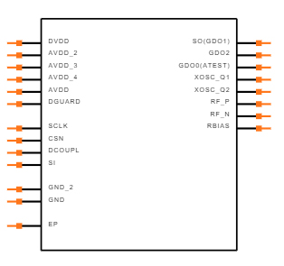
Pinout


Pin Number Pin Name Description
1 SCLK Serial configuration interface, clock input
2 SO (GDO1) Serial configuration interface, data output
Optional general output pin when CSn is high
3 GDO2 Digital output pin for general use:

• Test signals

• FIFO status signals

• Clear channel indicator

• Clock output, down-divided from XOSC

• Serial output RX data

4 DVDD 1.8 - 3.6 V digital power supply for digital I/O’s and for the digital core
voltage regulator
5 DCOUPL 1.6 - 2.0 V digital power supply output for decoupling
NOTE: This pin is intended for use with the CC1101 only. It can not be used
to provide supply voltage to other devices
6 GDO0
(ATEST)
Digital output pin for general use:

• Test signals

• FIFO status signals

• Clear channel indicator

• Clock output, down-divided from XOSC

• Serial output RX data

• Serial input TX data

Also used as analog test I/O for prototype/production testing
7 CSn Serial configuration interface, chip select
8 XOSC_Q1 Crystal oscillator pin 1, or external clock input
9 AVDD 1.8 - 3.6 V analog power supply connection
10 XOSC_Q2 Crystal oscillator pin 2
11 AVDD 1.8 - 3.6 V analog power supply connection
12 RF_P Positive RF input signal to LNA in receive mode
Positive RF output signal from PA in transmit mode
13 RF_N Negative RF input signal to LNA in receive mode
Negative RF output signal from PA in transmit mode
14 AVDD 1.8 - 3.6 V analog power supply connection
15 AVDD 1.8 - 3.6 V analog power supply connection
16 GND Analog ground connection
17 RBIAS External bias resistor for reference current
18 DGUARD Power supply connection for digital noise isolation
19 GND Ground connection for digital noise isolation
20 SI Serial configuration interface, data input

CC1101 CAD Model

Symbol

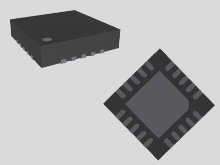
Footprint

3D Model

CC1101 Features

(1) RF Performance

• High sensitivity

o -116 dBm at 0.6 kBaud, 433 MHz, 1% packet error rate

o -112 dBm at 1.2 kBaud, 868 MHz, 1% packet error rate

• Low current consumption (14.7 mA in RX, 1.2 kBaud, 868 MHz)

• Programmable output power up to +12 dBm for all supported frequencies

• Excellent receiver selectivity and blocking performance

• Programmable data rate from 0.6 to 600 kbps

• Frequency bands: 300-348 MHz, 387-464 MHz and 779-928 MHz

(2) Analog Features

• 2-FSK, 4-FSK, GFSK, and MSK supported as well as OOK and flexible ASK shaping

• Suitable for frequency hopping systems due to a fast settling frequency synthesizer; 75 μs settling time

• Automatic Frequency Compensation (AFC) can be used to align the frequency synthesizer to the received signal centre frequency

• Integrated analog temperature sensor

(3) Digital Features

• Flexible support for packet-oriented systems; On-chip support for sync word detection, address check, flexible packet length, and automatic CRC handling

• Efficient SPI interface; All registers can be programmed with one “burst” transfer

• Digital RSSI output

• Programmable channel filter bandwidth

• Programmable Carrier Sense (CS) indicator

• Programmable Preamble Quality Indicator (PQI) for improved protection against false sync word detection in random noise

• Support for automatic Clear Channel Assessment (CCA) before transmitting (for listen-before-talk systems)

• Support for per-package Link Quality Indication (LQI)

• Optional automatic whitening and dewhitening of data

(4) Low-Power Features

• 200 nA sleep mode current consumption

• Fast startup time; 240 μs from sleep to RX or TX mode

• Wake-on-radio functionality for automatic low-power RX polling

• Separate 64-byte RX and TX data FIFOs (enables burst mode data transmission)

(5) General

• Few external components; Completely onchip frequency synthesizer, no external filters or switch needed

• Green package: RoHS compliant and no antimony or bromine

• Small size (QLP 4x4 mm package, 20 pins)

• Suited for systems targeting compliance with EN 300 220 (Europe) and FCC CFR Part 15 (US)

• Suited for systems targeting compliance with the Wireless MBUS standard EN 13757-4:2005

• Support for asynchronous and synchronous serial receive/transmit mode for backwards compatibility with existing radio communication protocols

Specifications

NA CC1101RGP technical specifications, attributes, parameters and parts with similar specifications to NA CC1101RGP.

undefined Tech Specifications

undefined undefined technical specifications, attributes, parameters and parts with similar specifications to undefined undefined.

Product Attribute Attribute Value
0 Products View Similar

CC1101 Functional Block Diagram

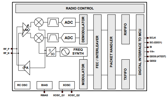
Functional Block Diagram


The image above shows a simplified block diagram of the CC1101. The CC1101 is equipped with a low-IF receiver. The low-noise amplifier (LNA) amplifies the received RF signal and converts it to the intermediate frequency in quadrature (I and Q) (IF). The  ADCs  digitize the I/Q signals at the IF. Digitally executed functions include automatic gain control (AGC), precise channel filtering, demodulation, and bit/packet synchronization.

The transmitter section of the CC1101 uses direct RF frequency synthesis.

In receive mode, the frequency synthesizer has an on-chip LC VCO and a 90-degree phase shifter for creating the I and Q LO signals for the down-conversion mixers. To XOSC Q1 and XOSC Q2, a crystal must be connected. The crystal oscillator generates the synthesizer's reference frequency as well as clocks for the ADC and digital section.

For configuration and data buffer access, a 4-wire SPI serial interface is employed. Channel setting, packet handling, and data buffering are all supported by the digital baseband.

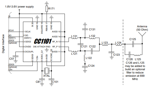
CC1101 Typical Application

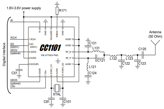
Typical Application and Evaluation Circuit 315/433 MHz (excluding supply decoupling capacitors)

Typical Application and Evaluation Circuit 868/915 MHz (excluding supply decoupling capacitors)

CC1101 Alternatives

Part Number Description Manufacturer
CC1100ERGPTTELECOMMUNICATION CIRCUITS Low-power Sub-1GHz wireless transceiver for China and Japan frequency bands 20-QFN -40 to 85 Texas Instruments
MD59-0049RTRTELECOMMUNICATION CIRCUITS RF and Baseband Circuit, PQCC20, 4 MM, PLASTIC, MLF-20 MACOM
CC1101RTKRG3TELECOMMUNICATION CIRCUITS IC TELECOM, CELLULAR, RF AND BASEBAND CIRCUIT, PQCC20, 4 X 4 MM, GREEN, PLASTIC, QLP-20, Cellular Telephone Circuit Texas Instruments
CC1101RTKTELECOMMUNICATION CIRCUITS TELECOM, CELLULAR, RF AND BASEBAND CIRCUIT, PQCC20, 4 X 4 MM, GREEN, PLASTIC, QLP-20 Texas Instruments
CC1101RTKG3TELECOMMUNICATION CIRCUITS TELECOM, CELLULAR, RF AND BASEBAND CIRCUIT, PQCC20, 4 X 4 MM, GREEN, PLASTIC, QLP-20 Texas Instruments

CC1101 Applications

• Ultra low-power wireless applications operating in the 315/433/868/915 MHz ISM/SRD bands

• Wireless alarm and security systems

• Industrial monitoring and control

• Wireless sensor networks

• AMR – Automatic Meter Reading

• Home and building automation

• Wireless MBUS


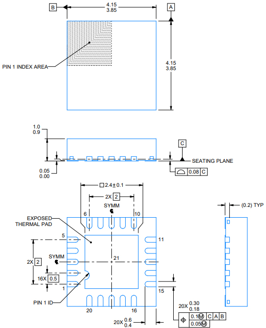
CC1101 Package

Package

CC1101 Manufacturer

Texas Instruments (TI), a multinational semiconductor business with operations in 35 countries, is first and foremost a reflection of its employees. We are problem-solvers cooperating to transform the world via technology, from the TIer who introduced the first functional integrated circuit in 1958 to the more than 30,000 TIers throughout the world today who develop, build, and distribute analog and embedded processor chips.

Datasheet PDF

undefined Documents

Download datasheets and manufacturer documentation for

Frequently Asked Questions

1.Which is easier to configure and use, CC1101 or SI4432?
The number of configuration registers required by CC1101 is far less than SI4432, and CC1101 can use the SmartRF Studio officially provided by TI for auxiliary configuration. So CC1101 is easier to configure and use than SI4432.
2.How to increase the anti-interference ability of CC1101?
433MHz is originally a straight line propagation, the anti-interference level is determined by the chip itself, and only other methods can be used to ensure the success rate of communication. For example: add a shielding cover to the hardware to isolate the power supply. The software protocol increases the preamble length, the synchronization word is allocated with 0x5A, 0xA5, or something, add the hardware address, software number, and add a CRC16. The interfered data packet is lost and retransmitted. The frequency offset bandwidth is narrowed a bit, the sensitivity is reduced, and then the communication rate is reduced, and the transmission power is increased.
3.What is the difference between CC1101 chip and CC1101-Q1?
The performance is the same, but the levels are different. CC1101 is an ordinary grade, and CC1101-Q is an automotive-grade, with a relatively wide operating temperature range.
4.The information of Arduino Uno chip (ATMEGA328P) and CC1101 based breadboard, what is an Arduino used for?
Arduino is an open-source electronics platform that uses simple hardware and software to make it easy to use. Arduino boards can take inputs - such as light from a sensor, a finger on a button, or a Twitter message - and convert them to outputs - such as turning on an LED, triggering a motor, or publishing anything online.
FAQ
1.Which is easier to configure and use, CC1101 or SI4432?
The number of configuration registers required by CC1101 is far less than SI4432, and CC1101 can use the SmartRF Studio officially provided by TI for auxiliary configuration. So CC1101 is easier to configure and use than SI4432.
2.How to increase the anti-interference ability of CC1101?
433MHz is originally a straight line propagation, the anti-interference level is determined by the chip itself, and only other methods can be used to ensure the success rate of communication. For example: add a shielding cover to the hardware to isolate the power supply. The software protocol increases the preamble length, the synchronization word is allocated with 0x5A, 0xA5, or something, add the hardware address, software number, and add a CRC16. The interfered data packet is lost and retransmitted. The frequency offset bandwidth is narrowed a bit, the sensitivity is reduced, and then the communication rate is reduced, and the transmission power is increased.
3.What is the difference between CC1101 chip and CC1101-Q1?
The performance is the same, but the levels are different. CC1101 is an ordinary grade, and CC1101-Q is an automotive-grade, with a relatively wide operating temperature range.
4.The information of Arduino Uno chip (ATMEGA328P) and CC1101 based breadboard, what is an Arduino used for?
Arduino is an open-source electronics platform that uses simple hardware and software to make it easy to use. Arduino boards can take inputs - such as light from a sensor, a finger on a button, or a Twitter message - and convert them to outputs - such as turning on an LED, triggering a motor, or publishing anything online.

TAGS

Share