ATTENTION: Due to increased demand and order volume, processing time may take an additional 1-3 business days.
HomeCommunitySubjectCD4007 CMOS Inverter: 14 SOIC Inverter, Pinout and Datasheet pdf [Video]

CD4007 CMOS Inverter: 14 SOIC Inverter, Pinout and Datasheet pdf [Video]

Logic - Specialty Logic 14-SOIC (0.154, 3.90mm Width) 3V~15V -40°C~85°C 4000B 4007 Complementary Pair Plus Inverter IC INVERTER COMP PR DUAL 14SOIC

346

Nov 22, 2021

Rock Christy

CMOS Inverter using CD4007 in a laboratory setting.

Logic - Specialty Logic 14-SOIC (0.154, 3.90mm Width) 3V~15V -40°C~85°C 4000B 4007 Complementary Pair Plus Inverter IC INVERTER COMP PR DUAL 14SOIC

CD4007 is a dual complementary pair plus inverter. This article is going to explain the pin, features, applications, datasheet, and more details about the CD4007 inverter.
 

CD4007CM

Inquiry
Min.: 1 Mult.: 1
Price not displayed? Not available to buy online? Please send an RFQ, and we will respond immediately.
Quick Links

What is CD4007?

The CD4007  is made up of three pairs of N - and P-channel enhancement mode MOS transistors that can be used in series or shunt applications. The IC works in a variety of environments and can interact with CMOSN  MOS, and TTL devices directly. The IC is suitable for a wide range of applications, including low thermal dissipation and noise immunity. The voltages at all pins must be kept between VSS  and VDD  at 0.3V at all times to ensure proper operation. Clamping diodes at VD and VSS  provide static protection for all inputs.

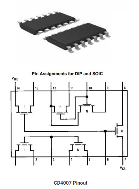
CD4007 Pinout

Pin No Pin Name Description
1 2Dp The drain of p Channel 2
2 2Sp Source of p Channel 2
3 2A Input Channel 2
4 2Sn Source of n Channel 2
5 2Dn The drain of n Channel 2
6 1A Input Channel 1
7 VSS Source Supply
8 1Dn The drain of n Channel 1
9 3Sn Source of n Channel 3
10 3A Input Channel 3
11 3Sp Source of p Channel 3
12 3Y output
13 1Dp The drain of p Channel 1
14 VDD Drain Supply

CD4007 CAD Model

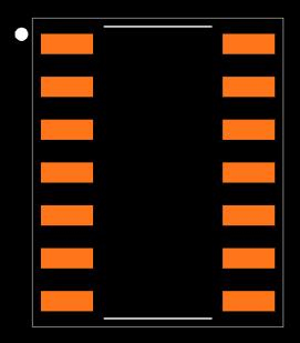
CD4007 Footprint

CD4007 3D Model

Specifications

ON Semiconductor CD4007CM technical specifications, attributes, parameters and parts with similar specifications to ON Semiconductor CD4007CM.

CD4007CM Tech Specifications

ON Semiconductor CD4007CM technical specifications, attributes, parameters and parts with similar specifications to ON Semiconductor CD4007CM.

Product Attribute Attribute Value
MountSurface Mount
Mounting TypeSurface Mount
Package / Case14-SOIC (0.154, 3.90mm Width)
Number of Pins14Pins
Supplier Device Package14-SOIC
Operating Temperature-40°C~85°C
PackagingTube
Series4000B
Published1999
Product Attribute Attribute Value
Part StatusObsolete
Moisture Sensitivity Level (MSL)1 (Unlimited)
Max Operating Temperature85°C
Min Operating Temperature-40°C
Supply Voltage3V~15V
Base Part Number4007
PolarityInverting
Number of Circuits2Circuits
Max Supply Voltage15V
Product Attribute Attribute Value
Min Supply Voltage3V
Number of Bits3Bits
Propagation Delay50 ns
Logic FunctionInverter
Logic TypeComplementary Pair Plus Inverter
Number of Input Lines3Input Lines
Number of Output Lines3Output Lines
RoHS StatusRoHS Compliant
Lead FreeLead Free
0 Products View Similar

CD4007 Features

  • Wide supply voltage range: 3.0V to 15V

  • High noise immunity: 0.45 VCC (Typ.)

  • 100% tested for quiescent current at 20V

  • Standardized symmetrical output characteristics

CD4007 Applications

  • Sharpers

  • Inverters

  • Threshold detectors

  • Linear amplifiers

  • Crystal oscillators

Using the CD4007 transistor array to make inverters

One CD4007 package can be used to make up to three separate inverters. The first one is the simplest to set up, as illustrated below, by connecting pins  8 and 13 as the inverter output. The input will be on pin  6. Make sure pin14 VDD  is connected to power and pin 7 VSS  is connected to the ground.

CD4007 Inverter

Pin 2 is connected to VDD.  pin  4 to VSS.  Pins 1 and 5 are connected as the output, and pin  3 is used as the input in the second inverter. Pin11 is connected to VDDpin 9 to VSSpin 12 is the output, and pin  10 is the input in the third inverter.

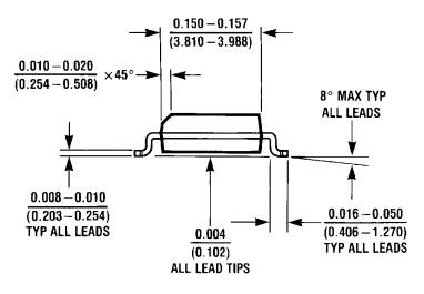
CD4007 Dimensions

CD4007 Dimensions

CD4007 Manufacturer

ON Semiconductor (Nasdaq: ON) is driving energy-efficient innovations, empowering customers to reduce global energy use. The company offers a comprehensive portfolio of energy-efficient power and signal management, logic, discrete and custom solutions to help design engineers solve their unique design challenges in automotive, communications, computing, consumer, industrial, LED lighting, medical, military/aerospace, and power supply applications.  ON Semiconductor operates a responsive, reliable, world-class supply chain and quality program, and a network of manufacturing facilities, sales offices, and design centers in key markets throughout North America, Europe, and the Asia Pacific regions.

Datasheet PDF

Download datasheets and manufacturer documentation for ON Semiconductor CD4007CM.

CD4007CM Documents

Download datasheets and manufacturer documentation for CD4007CM

Frequently Asked Questions

What can be CD4007 used for?
The CD4007 is a very versatile IC with many uses. For example, a single CD4007 can be used to make a chain of 3 inverters, an inverter plus two transmission gates, or a complex logic gate. Inverters and transmission gates are particularly useful for building D flip-flops.
What is the voltage of CD4007?
The IC offers a wide variety of applications such as low thermal dissipation and high noise immunity. For proper operation, the voltages at all pins must be constrained to be between VSS at 0.3V and VDD at 0.3V at all times.
What is the circuit of CD4007?
The CD4007 is a monolithic integrated circuit fabricated in Metal Oxide Semiconductor technology available in DIP and SOP packages. The CD4007 (HCF4007UB) type is comprised of three n-channel and three p-channel enhancement type MOS transistors.
FAQ
What can be CD4007 used for?
The CD4007 is a very versatile IC with many uses. For example, a single CD4007 can be used to make a chain of 3 inverters, an inverter plus two transmission gates, or a complex logic gate. Inverters and transmission gates are particularly useful for building D flip-flops.
What is the voltage of CD4007?
The IC offers a wide variety of applications such as low thermal dissipation and high noise immunity. For proper operation, the voltages at all pins must be constrained to be between VSS at 0.3V and VDD at 0.3V at all times.
What is the circuit of CD4007?
The CD4007 is a monolithic integrated circuit fabricated in Metal Oxide Semiconductor technology available in DIP and SOP packages. The CD4007 (HCF4007UB) type is comprised of three n-channel and three p-channel enhancement type MOS transistors.

TAGS

Share