ATTENTION: Due to increased demand and order volume, processing time may take an additional 1-3 business days.
HomeCommunitySubjectCD4013 Dual D Flip-Flop: Circuits, Flip Datasheet pdf and Equivalents

CD4013 Dual D Flip-Flop: Circuits, Flip Datasheet pdf and Equivalents

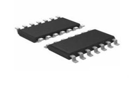
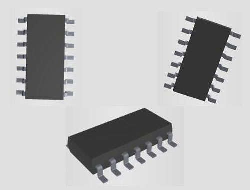
Logic - Flip Flops 15.5MHz 14-SOIC (0.154, 3.90mm Width) 3V~15V -55°C~125°C TA 4000B 15.5MHz 4013 5pF 4000 CMOS, SMD, 4013, SOIC14, 15V

394

Oct 31, 2021

Theobald Lizzie

CD4013 | 7474 | Dual D type Flip Flops | Divide by 2 Counter | Theory & Practical

Logic - Flip Flops 15.5MHz 14-SOIC (0.154, 3.90mm Width) 3V~15V -55°C~125°C TA 4000B 15.5MHz 4013 5pF 4000 CMOS, SMD, 4013, SOIC14, 15V

The CD4013 dual D flip-flop is a monolithic complementary MOS (CMOS) integrated circuit constructed with N- and P-channel enhancement mode transistors. This article will explain datasheet pdf, circuits, pinout, equivalents, applications, and other details about CD4013 dual d flip-flop.
CD4013BCM

2308In Stock
Min.: 1 Mult.: 1
Price not displayed? Not available to buy online? Please send an RFQ, and we will respond immediately.
Quick Links

Overview of Dual D Flip-Flop

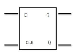
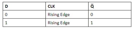
A digital electrical circuit called a D (or Postpone) Flip Flop (Figure 1) is used to delay the change of state of its output signal (Q) until the next rising edge of a clock timing input signal occurs.

A D-type latch operates with a delay in input by one clock cycle. Thus, by cascading many D-type flip-flops delay circuits can be created, which are used in many applications such as in digital television systems.

D Flip-Flop

Truth Table

The D flip flop is the most important flip flop from other clocked types. It ensures that at the same time, both the inputs, i.e., S and R, are never equal to 1. The Delay flip-flop is designed using a gated SR flip-flop with an inverter connected between the inputs allowing for a single input D (Data).

What is CD4013?

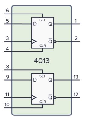
The CD4013 device consists of two identical, independent data-type flip-flops. Each flip-flop has independent data, set, reset, and clock inputs and Q and Q outputs. A monolithic complementary MOS (CMOS) integrated circuit containing N- and P-channel enhancement mode transistors, the CD4013 dual D flip-flop is a monolithic complementary MOS (CMOS) integrated circuit. Data, set, reset, and clock inputs, as well as "Q" and "Q" outputs, are all independent on each flip-flop.

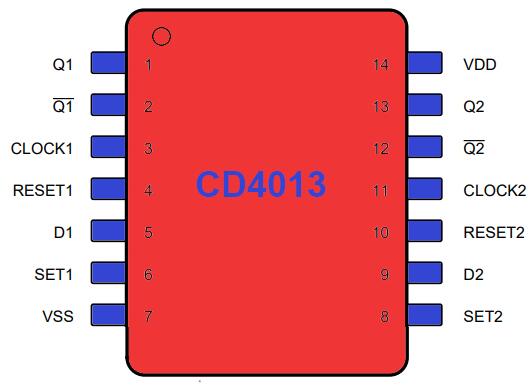
CD4013 Pinout

CD4013 Pinout


Pin   Number Pin Name Pin Description
14 VDD Supply voltage input,   5V to 15V
7 VSS Ground reference
1, 2 INPUT AND gate one input
3 OUTPUT AND gate one output
5, 6 INPUT AND gate two inputs
4 OUTPUT AND gate two output
8, 9 INPUT AND gate three inputs
10 OUTPUT AND gate three output
12, 13 INPUT AND gate four inputs
11 OUTPUT AND gate four output

CD4013 CAD Model

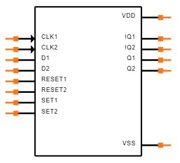
CD4013 Symbol

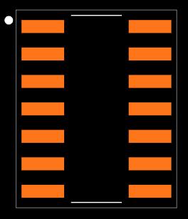
CD4013 Footprint

CD4013 3D Model

Specifications

CD4013BCM Tech Specifications

ON Semiconductor CD4013BCM technical specifications, attributes, parameters and parts with similar specifications to ON Semiconductor CD4013BCM.

Product Attribute Attribute Value
MountSurface Mount
Mounting TypeSurface Mount
Package / Case14-SOIC (0.154, 3.90mm Width)
Number of Pins14Pins
Supplier Device Package14-SOIC
Clock-Edge Trigger TypePositive Edge
Number of Elements2 Elements
Operating Temperature-55°C~125°C TA
PackagingTube
Series4000B
Published2002
Part StatusObsolete
Moisture Sensitivity Level (MSL)1 (Unlimited)
TerminationSMD/SMT
TypeD-Type
Max Operating Temperature125°C
Product Attribute Attribute Value
Min Operating Temperature-55°C
Voltage - Supply3V~15V
Frequency15.5MHz
Base Part Number4013
FunctionSet(Preset) and Reset
Output TypeDifferential
PolarityNon-Inverting
Voltage18V
Number of Circuits2Circuits
Max Supply Voltage15V
Min Supply Voltage3V
Output Current8.8mA
Number of Bits2Bits
Clock Frequency15.5MHz
Propagation Delay350 ns
Turn On Delay Time65 ns
Product Attribute Attribute Value
Logic FunctionAND, D-Type, Flip-Flop
Current - Quiescent (Iq)4μA
Number of Inputs1Input
Number of Gates2Gates
Number of Bits per Element1
Max Propagation Delay @ V, Max CL120ns @ 15V, 50pF
Trigger TypePositive Edge
High Level Output Current-4.2mA
Input Capacitance5pF
Low Level Output Current4.2mA
Number of Input Lines1Input Line
Number of Output Lines1Output Line
REACH SVHCNo SVHC
RoHS StatusRoHS Compliant
Lead FreeLead Free
0 Products View Similar

CD4013 Features

  • Asynchronous Set-Reset Capability

  • Static Flip-Flop Operation

  • Medium-Speed Operation: 16 MHz (Typical) Clock Toggle Rate at 10-V Supply

  • Standardized Symmetrical Output Characteristics

  • Maximum Input Current Of 1-µA at 18 V over Full Package Temperature Range: 100 nA at 18 V and 25°C

  • Wide supply voltage range: 3.0V to 15V.

  • High noise immunity: 0.45 VDD (Typ.)

  • Low power TTL: fan out of 2 driving 74L.

  • Compatibility: or 1 driving 74LS.

CD4013 Applications

  • Power Delivery

  • Grid Infrastructure

  • Medical, Healthcare, and Fitness

  • Body Electronics and Lighting

  • Building Automation

  • Telecom Infrastructure

  • Test and Measurement

CD4013 Circuit

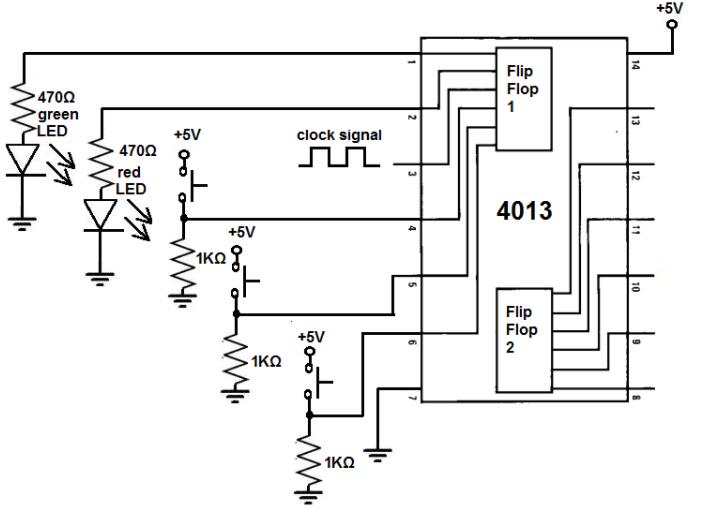
To power the 4013, we connect VSS, pin 8, to ground and feed 5V to VDD, pin 16.

A clock signal is connected to the 4013's clock, which is pin 3. We connect a clock signal to the clock of the 4013, which is pin 3. This clock pin can be obtained from several sources such as a frequency generator or a 555 timer chip or a 4046 chip. It can even be obtained from a 7414 Schmitt trigger inverter chip.

A pull-down resistor is connected to each of the three input pins, the data pin, set pin, and reset pin. When the pushbutton is not pressed, the pin is generally in the LOW condition. When we press down on the pushbutton, it switches to HIGH mode. So all the pins have a value of 0 at first, but when we press the pushbutton, it changes to a value of 1.

CD4013 Circuit

How to use CD4013?

You must first connect the VDD pin to the positive supply terminal and the GND pin to the negative supply terminal before using any of the D flip-flops gates in the device.

A power supply voltage of 3V to 15V can be used. The 4013 chip supports up to 20V in some versions. For accurate values, consult the datasheet for your chip's version.

CD4013 Diagram

The D (data) pin is where you input the data you want to store in the flip-flop.

Provide a signal that goes from LOW to HIGH on the CLK pin to store the data from the D pin to the output pin Q.

The output pin Q is always the opposite of pin Q.

Use the S (set) pin to force the output pin HIGH.

Use the R (reset) pin to force the output pin LOW.

Alternatives for CD4013 D Flip Flop

4174: Hex D-type Flip-Flop

4175: Quad D-type Flip-Flop

40174: Hex D-type Flip-Flop

40175: Quad D-type Flip-Flop

74HC74: Dual D-type Flip-Flop

74HC79: Dual D-type Flip-Flop

CD4013 Dimensions

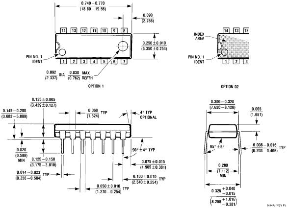
CD4013 Dimensions

CD4013 Manufacturer

On Semiconductor (Nasdaq: ON) is a manufacturer engaging itself in reducing energy use. It features a comprehensive portfolio of power, signal management, and logic, custom solutions that are energy efficient. It acts as a world-class supply chain with high reliability and a network of manufacturing facilities, sales, offices, and design centers in key markets through North America, Europe, and the Asia Pacific regions.

Frequently Asked Questions

How does CD4013 work?
The 4013 contains two independent D-type flip-flops with asynchronous set/reset inputs. Whenever the set or reset pins go high, the appropriate output is expressed immediately on the outputs. When set and reset are low, the output shows the data at the input at the time of the last low-to-high clock transition.
What is CD4013 used for?
The CD4013 or IC-4013 is a CMOS logic chip with two D-Type (DATA) Flip-flops. A clock pulse flow to C (clock pin), will store the data at the D input. Connect clock and both Q output to make a toggle flip-flop for counting.
What is clock signal in flip flops?
A clock pulse is a time-varying voltage signal applied to control the operation (triggering) of a flip flop. For example, if a clock pulse is of frequency 1 Hz, the voltage it will supply will oscillate between X Volts and Y Volts(X and Y are any dc voltages), and this change occurs every half second.
What happens if flip-flop has no clock?
Flip flops are memory devices and clocks are used so that they respond to external stimuli. When the clock is active only then the changes in the input will be registered. So, if you permanently disable the clock, the flip flop will permanently retain the previous input.
Is D flip-flop edge triggered?
The D flip-flop is an edge-triggered device that transfers input data to Q on a clock rising or falling edge. Data Latches are level-sensitive devices such as the data latch and the transparent latch.
FAQ
How does CD4013 work?
The 4013 contains two independent D-type flip-flops with asynchronous set/reset inputs. Whenever the set or reset pins go high, the appropriate output is expressed immediately on the outputs. When set and reset are low, the output shows the data at the input at the time of the last low-to-high clock transition.
What is CD4013 used for?
The CD4013 or IC-4013 is a CMOS logic chip with two D-Type (DATA) Flip-flops. A clock pulse flow to C (clock pin), will store the data at the D input. Connect clock and both Q output to make a toggle flip-flop for counting.
What is clock signal in flip flops?
A clock pulse is a time-varying voltage signal applied to control the operation (triggering) of a flip flop. For example, if a clock pulse is of frequency 1 Hz, the voltage it will supply will oscillate between X Volts and Y Volts(X and Y are any dc voltages), and this change occurs every half second.
What happens if flip-flop has no clock?
Flip flops are memory devices and clocks are used so that they respond to external stimuli. When the clock is active only then the changes in the input will be registered. So, if you permanently disable the clock, the flip flop will permanently retain the previous input.
Is D flip-flop edge triggered?
The D flip-flop is an edge-triggered device that transfers input data to Q on a clock rising or falling edge. Data Latches are level-sensitive devices such as the data latch and the transparent latch.

TAGS

Share