CD4017 CD4015 LED Chaser Circuit
IC, 4BIT SIPO SHIFT REGISTER, DIP-16
The CD4015 is a Dual 4-bit Shift Register. It has a wide operating voltage of up to 18V. So this article is going to talk about more detailed information about CD4015.

IC, 4BIT SIPO SHIFT REGISTER, DIP-16 The CD4015 is a Dual 4-bit Shift Register. It has a wide operating voltage of up to 18V. So this article is going to talk about more detailed information about CD4015.
912
Mar 15, 2022
Ted Esther
CD4017 CD4015 LED Chaser Circuit
IC, 4BIT SIPO SHIFT REGISTER, DIP-16
The CD4015 is a Dual 4-bit Shift Register. It has a wide operating voltage of up to 18V. So this article is going to talk about more detailed information about CD4015.
CD4015BE
| Quantity | Unit Price | Ext. Price |
|---|---|---|
| 1+ | $2.61844 | $2.62 |
| 10+ | $2.47023 | $24.7 |
| 100+ | $2.33041 | $233.04 |
| 500+ | $2.1985 | $1099.25 |
| 1000+ | $2.07405 | $2074.05 |
A CMOS IC with two 4-bit shift registers is the CD4015. There are serial input and parallel output pins on each shift register. It's widely used to provide a microcontroller, such as Arduino, extra output pins. A Dual 4-bit Shift Register is the CD4015. It has a wide operating voltage range of up to 18V, making it suitable for high-voltage applications. The IC is typically used in conjunction with a microcontroller as an I/O expander to control various outputs such as LEDs and LCD displays.
Shift register with dual 4-bit serial input and parallel output.
3V to 18V operating voltage
80uA Power Consumption
8.5MHz @15V Clock Input Frequency
Clock Frequency Maximum: 12Mhz @10V
16-pin PDIP, GDIP, and PDSO packages are available.
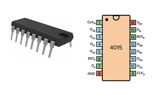
CD4015 Pinout
| Pin Name | Pin # | Type | Description |
| VDD | 16 | Power | Supply Voltage (+3 to +15V) |
| GND | 8 | Power | Ground (0V) |
| D A | 7 | Input | Data pin for register A |
| CLK A | 9 | Input | Clock pulse for register A |
| RST A | 6 | Input | Reset pin for register A |
| Q A0 ,Q A1 ,Q A2 ,Q A3 | 2,3,4,5 | Output | 4-bit output for register A |
| D B | 15 | Input | Data pin for register B |
| CLK B | 1 | Input | Clock pulse for register B |
| RST B | 14 | Input | Reset pin for register B |
| Q B0 ,Q B1 ,Q B2 ,Q B3 | 10,11,12,13 | Output | 4-bit output for register B |
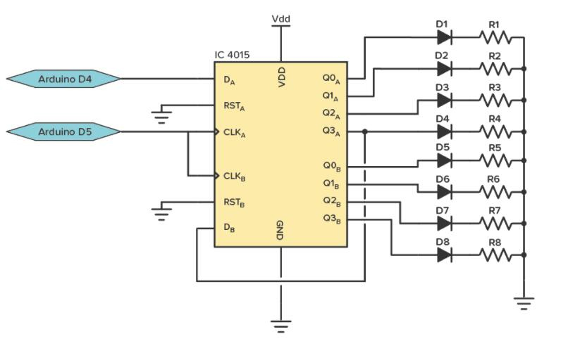
CD4015 Circuit
Texas Instruments CD4015BE technical specifications, attributes, parameters and parts with similar specifications to Texas Instruments CD4015BE.
| Product Attribute | Attribute Value | |
|---|---|---|
| Lifecycle Status | ACTIVE (Last Updated: 4 days ago) | |
| Factory Lead Time | 8 Weeks | |
| Contact Plating | Gold | |
| Mount | Through Hole | |
| Mounting Type | Through Hole | |
| Package / Case | 16-DIP (0.300, 7.62mm) | |
| Number of Pins | 16Pins | |
| Weight | 951.693491mg | |
| Number of Elements | 2 Elements | |
| Operating Temperature | -55°C~125°C | |
| Packaging | Tube | |
| Series | 4000B | |
| JESD-609 Code | e4 | |
| Part Status | Active | |
| Moisture Sensitivity Level (MSL) | 1 (Unlimited) | |
| Number of Terminations | 16Terminations | |
| ECCN Code | EAR99 |
| Product Attribute | Attribute Value | |
|---|---|---|
| Voltage - Supply | 3V~18V | |
| Terminal Position | DUAL | |
| Supply Voltage | 5V | |
| Frequency | 17MHz | |
| Base Part Number | CD4015 | |
| Function | Serial to Parallel | |
| Output Type | Push-Pull | |
| Supply Voltage-Min (Vsup) | 3V | |
| Load Capacitance | 50pF | |
| Power Dissipation | 500mW | |
| Propagation Delay | 400 ns | |
| Quiescent Current | 100μA | |
| Turn On Delay Time | 400 ns | |
| Logic Function | Shift Register | |
| Direction | Unidirectional | |
| Logic Type | Shift Register | |
| Output Polarity | TRUE |
| Product Attribute | Attribute Value | |
|---|---|---|
| Number of Bits per Element | 4Bits per Elements | |
| Trigger Type | POSITIVE EDGE | |
| Input Capacitance | 5pF | |
| Schmitt Trigger | No | |
| Power Supply Current-Max (ICC) | 0.3mA | |
| Number of Input Lines | 1Input Line | |
| fmax-Min | 8.5 MHz | |
| Height | 5.08mm | |
| Length | 19.3mm | |
| Width | 6.35mm | |
| Thickness | 3.9mm | |
| REACH SVHC | No SVHC | |
| Radiation Hardening | No | |
| RoHS Status | ROHS3 Compliant | |
| Lead Free | Lead Free |
A shift register is a simple memory circuit capable of storing a large number of bits. A sequence of flip-flops can be used to make one. One bit can be stored in each flip-flop. A 4-bit shift register, such as the ones found in the CD4015 chip, has four flip-flops and is commonly referred to as a 4-stage shift register:
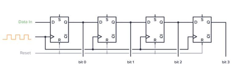
Whatever is on the Data In pin after the first clock pulse is stored in the first flip-flop. What was previously stored on the first flip-flop is now stored on the second flip-flop. What was formerly kept on the second flip-flop is now stored on the third... And so forth.
The bit saved on the previous flip-flop will be overwritten. As a result, every clock pulse shifts the data one flip-flop (or one position) to the right. As a result, the moniker "shift register" was coined.
To begin, connect the positive supply terminal to the VDD pin and the negative supply terminal to the GND pin. A power supply voltage of 3V to 15V can be used. Some variants of the 4015 IC, however, can handle up to 20V. For accurate values, consult your datasheet.
Each of the chip's two shift registers has its own Clock, Reset, and Data pins. To load data into the registers, use the clock and data pins as follows: Whatever is on the D pin is transferred into the register on each rising edge of the CLK pin.
Set the RST pin to HIGH to reset the register's four bits to 0000. Otherwise, keep it to a minimum.
The state of the shift registers can be read from the Qxx pins at any moment.
CD4015
NTE4015
MC14015
HCF4015
LTC4015
TC4015
HEF4015
Expand the GPIO pin on an MCU/MPU
LED Matrix/Cube Projects
Interface LCD
Cascading applications
High logic level controller
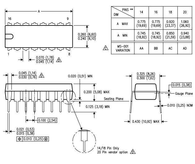
CD4015 Package information
Major Brands is one of Jameco's primary suppliers, offering the most popular name brand components. We stand behind anything we sell. We only sell high-quality, dependable products and strive to meet or surpass industry standards. The items are in stock and ready to ship. For almost 45 years, Jameco has been assisting makers and manufacturers with everything from design to delivery.
Download datasheets and manufacturer documentation for CD4015BE
TAGS
Comments