ATTENTION: Due to increased demand and order volume, processing time may take an additional 1-3 business days.
HomeCommunitySubjectCD4027 JK Flip-Flop IC:Pinout, Diagram and Datasheet

CD4027 JK Flip-Flop IC:Pinout, Diagram and Datasheet

TEXAS INSTRUMENTS CD4027BM Flip-Flop, Master/Slave, Complementary Output, Differential, Positive Edge, JK, 45 ns, 24 MHz

3594

Aug 10, 2021

Basil Katte

CD4027 based 4 bit up counter simulation in Proteus


TEXAS INSTRUMENTS CD4027BM Flip-Flop, Master/Slave, Complementary Output, Differential, Positive Edge, JK, 45 ns, 24 MHz

CD4027 is a dual package JK flip-flop IC. This article mainly introduce pinout,diagram, datasheet and other detailed information about Texas Instruments CD4027.

CD4027BM

309In Stock
Min.: 1 Mult.: 1
Quantity Unit Price Ext. Price
1+ $1.629$1.63
10+ $1.5368$15.37
100+ $1.44981$144.98
500+ $1.36774$683.87
1000+ $1.29032$1290.32
Unit Price:$1.629
Subtotal: $1.63
Looking for a better price? Want a lower wholesale price? Please send an RFQ, and we will respond immediately.
Quick Links

CD4027 Description

CD4027 is a CMOS based high voltage high speed Dual JK Flip-Flop that is generally used for data storing. The Flip-Flop could typically operate at a speed of 16MHz even at high voltages like 15V with a low noise margin of only 2.5V. 

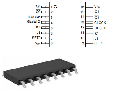
Two similar or equal JK flip flops are contained in the IC. Each pair of JK flip flop with IC  has provision of pins J, K, set, reset along with clock and with two output terminals which are complimentary of each other. 

JK flip flop can be employed in the applications like voice register, counters or else as a control circuit.

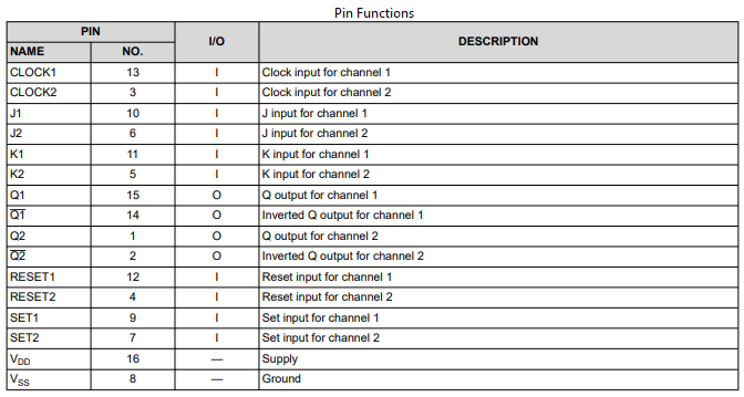
CD4027 Pinout

CD4027 CAD Model

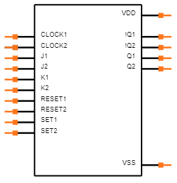
Symbol


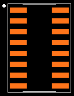
Footprint


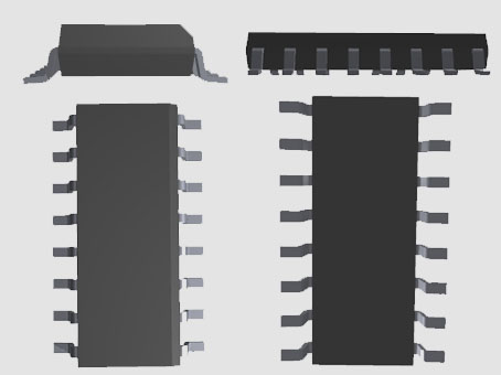
3D Model

CD4027 Features

●Dual JK Flip Flop Package IC

●Operating Speed: 16MHz( medium speed)

●Operating Voltage: 5V, 10V, 15V

●Maximum Operating Voltage: 20V

●Input Rise/Fall time at 5V : 45us

●Minimum High Level Input Voltage: 2 V

●Maximum Low Level Input Voltage: 0.8 V

●Available in 14-pin PDIP, GDIP, PDSO packages

●Static Flip-Flop Operation retains state indefinitely

●High noise immunity of 0.45 VDD(typ.)

●Set and Reset capability

●TTL compatible

●Low power of 50 nW (typ.)

●Set-reset capability

●With clock level either high or low

●Toggle rate at 10 V

●Standardized symmetrical output characteristics

●100% tested for quiescent current at 20 V

●Maximum input current of 1 μA at 18 V over full package-temperature range; 100 nA at 18 V and 25°C

●Noise margin (over full package-temperature range):

– 1 V at VDD = 5 V

– 2 V at VDD = 10 V

– 2.5 V at VDD = 15 V

Specifications

Texas Instruments CD4027BM technical specifications, attributes, parameters and parts with similar specifications to Texas Instruments CD4027BM.

CD4027BM Tech Specifications

Texas Instruments CD4027BM technical specifications, attributes, parameters and parts with similar specifications to Texas Instruments CD4027BM.

Product Attribute Attribute Value
Lifecycle StatusACTIVE (Last Updated: 3 days ago)
Factory Lead Time6 Weeks
Contact PlatingGold
MountSurface Mount
Mounting TypeSurface Mount
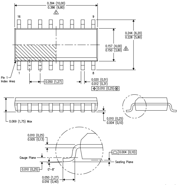
Package / Case16-SOIC (0.154, 3.90mm Width)
Number of Pins16Pins
Weight141.690917mg
Clock-Edge Trigger TypePositive Edge
Operating Temperature-55°C~125°C TA
PackagingTube
Series4000B
JESD-609 Codee4
Pbfree Codeyes
Part StatusActive
Moisture Sensitivity Level (MSL)1 (Unlimited)
Number of Terminations16Terminations
ECCN CodeEAR99
Product Attribute Attribute Value
TypeJK Type
Voltage - Supply3V~18V
Terminal PositionDUAL
Terminal FormGULL WING
Peak Reflow Temperature (Cel)260
Supply Voltage5V
Base Part NumberCD4027
FunctionSet(Preset) and Reset
Output TypeDifferential
PolarityNon-Inverting
Supply Voltage-Min (Vsup)3V
Number of Channels2Channels
Load Capacitance50pF
Output Current6.8mA
Clock Frequency24MHz
Propagation Delay300 ns
Quiescent Current20μA
Turn On Delay Time45 ns
Product Attribute Attribute Value
Logic FunctionAND, Flip-Flop, JK-Type
Current - Quiescent (Iq)4μA
Number of Bits per Element1
Max Propagation Delay @ V, Max CL90ns @ 15V, 50pF
Trigger TypePositive Edge
Input Capacitance5pF
Power Supply Current-Max (ICC)0.06mA
Max Frequency@Nom-Sup3500000Hz
Height1.75mm
Length9.9mm
Width3.91mm
Thickness1.58mm
REACH SVHCNo SVHC
Radiation HardeningNo
RoHS StatusROHS3 Compliant
Lead FreeLead Free
0 Products View Similar

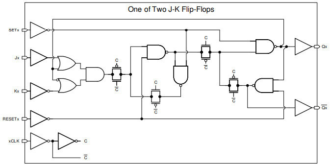
CD4027 Functional Block Diagram

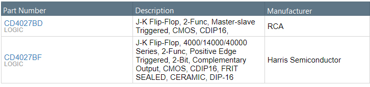
CD4027 Alternatives

Where to use CD4027?

The CD4027 is a dual in-line JK flip flop IC. Meaning it has two JK flip flops inside it and each can be used individually based on our application. The term JK flip flop comes after its inventor Jack Kilby. 


The JK flip flops are considered to be the most efficient flip-flop and can be used for certain applications on its own. The flip-flops are also called as latching devices meaning it can remember one single bit of data and latch the output based on it, due to this property they are commonly used as shift registers, control registers, storage registers or where ever a small memory is required. 


More than one Flip Flop can be used in series to act as an EEPROM for holding small amount of data. The JK flip flop is considered to be more suitable for practical application because of its truth table that is the output of the flip flop will be stable for all types of inputs.


So if you are looking for a IC for latching purpose or to act as a small programmable memory for you project then this IC might be the right choice for you.

How to use CD4027?

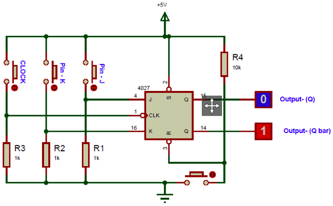
As told earlier we have two JK flip flops in this IC, the IC is powered by +5V typically the minimum and maximum input and output voltage for the input (J,K) pins and the output (Q, Q bar) pins are discussed in the specifications above. The below circuit shows a typical sample connection for the JK flip-flop.

The J and K pins are the input pins for the Flip-Flop and the Q and Q bar pins are the output pins. Note that the input pins are pulled down to ground through a 1k resistor or less, this way we can avoid the pin in floating condition. That is the pin will held to ground when the button is not pressed and when the button is pressed the pin will be held to supply voltage.


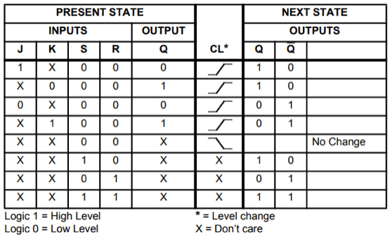
The reset button should be pulled up through a 1K resistor and when grounded will reset the flip-flop. The clock signal for the JK flip-flop is responsible for changing the state of the output. The flip-flop will change its output only during the rising edge of the clock signal. The clock signal here is just a push button but can be type of pulse like a PWM signal. The output state of the flip flops can be determined form the truth table below.

Normally during regular operation of the IC the reset pin will be set high and the clock pulse of known frequency will be supplied to the clock pin, then the value o J and K will be varied based on the input signals and the respective output will be obtained on the Q and Q bar pins. This region of operation in highlighted in red colour on the Truth table above.


CD4027 Applications

●Shift Registers

●Voice registers and Memory or Control Registers

●EEPROM circuits

●Latching devices

●Registers, control circuits,Latching devices and Counters

●Computer memory circuits

CD4027 Package

CD4027 Manufacturer

Texas Instruments (TI) is an American technology company headquartered in Dallas, Texas, which designs and manufactures semiconductors and various integrated circuits, and sells them to electronic designers and manufacturers worldwide. It is one of the top 10 semiconductor companies in global sales. The company focuses on the development of analog chips and embedded processors, which account for more than 80% of its revenue. TI also produces TI digital light processing technology and educational technology products, including calculators, microcontrollers and multi-core processors. As of 2016, the company has 45,000 patents worldwide.

Datasheet PDF

Download datasheets and manufacturer documentation for Texas Instruments CD4027BM.

CD4027BM Documents

Download datasheets and manufacturer documentation for CD4027BM

Frequently Asked Questions

1.What is the difference between CD4027 and 74LS112? Which circuit is better for the two?
(1). CD4027 is a CMOS device with a wide operating power supply voltage range (3V~18V), while 74LS112 is a TTL device, which can only work within the voltage range of 5V±0.5V; (2). CD4027 is a rising edge trigger, and 74LS112 is a falling edge trigger; (3). The delay time of 74LS is much smaller than that of CD4027; (4). CD4027 has higher input impedance, larger fan-out coefficient and lower power consumption, while 74LS112 has stronger drive capability; (5). The order of their pins is also different. According to the above-mentioned respective characteristics, select the application occasions. For example, if the working voltage is only about 3V or higher than 6V, choose CD4027; when working at about 5V and hope to have a stronger driving ability, choose 74LS112.
2.Is there any difference between CD4027 in-line and patch? What's the difference?
The chip packaging form is different, the pin position and function are the same.
3.What circuit is composed of electronic circuit CD4027?
CD4027 contains two independent, complementary and symmetrical J-K master-slave flip-flop monolithic integrated circuits. Each flip-flop provides J, K, set, reset, clock input, and buffered Q and Q non-output signals. This device can be used as a shift register, and by connecting the Q output to the data input, it can be used as a counter and flip-flop. When the rising edge of the clock triggers, the logic level added to the D input terminal is transferred to the Q output terminal. Set and reset have nothing to do with the clock, but are completed by the high level on the set or reset line respectively.
FAQ
1.What is the difference between CD4027 and 74LS112? Which circuit is better for the two?
(1). CD4027 is a CMOS device with a wide operating power supply voltage range (3V~18V), while 74LS112 is a TTL device, which can only work within the voltage range of 5V±0.5V; (2). CD4027 is a rising edge trigger, and 74LS112 is a falling edge trigger; (3). The delay time of 74LS is much smaller than that of CD4027; (4). CD4027 has higher input impedance, larger fan-out coefficient and lower power consumption, while 74LS112 has stronger drive capability; (5). The order of their pins is also different. According to the above-mentioned respective characteristics, select the application occasions. For example, if the working voltage is only about 3V or higher than 6V, choose CD4027; when working at about 5V and hope to have a stronger driving ability, choose 74LS112.
2.Is there any difference between CD4027 in-line and patch? What's the difference?
The chip packaging form is different, the pin position and function are the same.
3.What circuit is composed of electronic circuit CD4027?
CD4027 contains two independent, complementary and symmetrical J-K master-slave flip-flop monolithic integrated circuits. Each flip-flop provides J, K, set, reset, clock input, and buffered Q and Q non-output signals. This device can be used as a shift register, and by connecting the Q output to the data input, it can be used as a counter and flip-flop. When the rising edge of the clock triggers, the logic level added to the D input terminal is transferred to the Q output terminal. Set and reset have nothing to do with the clock, but are completed by the high level on the set or reset line respectively.

TAGS

Share