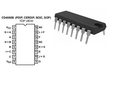
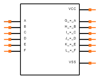
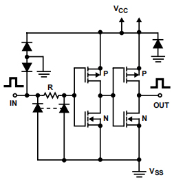
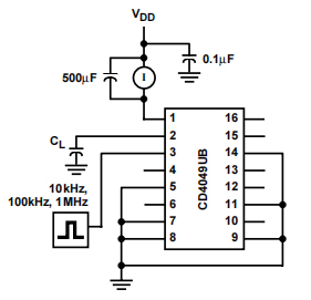
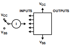
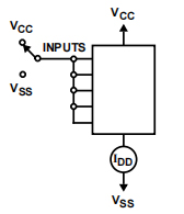
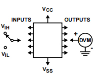
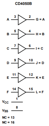
CD4050 device is nverting and the non-inverting hexadecimal buffers each have a logic level conversion function using only one power supply voltage (VCC). This input signal high level (VIH) may exceed the VCC power supply This device are used for logic level voltage Conversion. This device are designed to be used as CMOS To DTL/TTL converter, can directly drive two DTL/TTL load. (VCC = 5V, VOL ≤ 0.4V, IOL ≥ 3.3mA.) CD4050 is designated as replace CD4009UB and CD4010B respectively. Because CD4049UB and CD4050B only need one power supply, they are better than CD4009UB and CD4010B, should be used instead of CD4009UB And CD4010B in all inverters, current drivers or logic levels convert the application. In these applications CD4049UB and CD4050B are pin compatible CD4009UB and CD4010B are respectively Replace these devices in existing and new devices design. Terminal 16 is not connected internally CD4049UB or CD4050B, so connect to this
The terminals have no effect on the operation of the circuit. in order to applications that do not require high sink current or voltage For conversion, it is recommended to use CD4069UB hexadecimal inverter.