ATTENTION: Due to increased demand and order volume, processing time may take an additional 1-3 business days.
HomeCommunitySubjectCD4052 4-Channel Multiplexer and Demulitplexer IC: Datasheet, Equivalent and Working

CD4052 4-Channel Multiplexer and Demulitplexer IC: Datasheet, Equivalent and Working

Interface - Analog Switches, Multiplexers, Demultiplexers 16-SOIC (0.154, 3.90mm Width) 240Ohm -55°C~125°C TA 4052 1.05kOhm 4000 CMOS, SMD, 4052, SOIC16, 15V

228

Oct 14, 2021

Olive Walter

Interface - Analog Switches, Multiplexers, Demultiplexers 16-SOIC (0.154, 3.90mm Width) 240Ohm -55°C~125°C TA 4052 1.05kOhm 4000 CMOS, SMD, 4052, SOIC16, 15V

The CD4052 is a 4-Channel Multiplexer and Demultiplexer IC. It can either be used as a 4:1 Multiplexer or 1:4 Demultiplexer. This article mainly covers datasheet, equivalents, pin, working, and more details about CD4052 multiplexer. Furthermore, there is a huge range of semiconductors, capacitors, resistors, and ICs in stock. Welcome your RFQ!

CD4052BCM

14In Stock
Min.: 1 Mult.: 1
Price not displayed? Not available to buy online? Please send an RFQ, and we will respond immediately.
Quick Links

What is CD4052 Multiplexer?

The CD4052 is a 4-channel analog/digital dual single-pole switch that can be used in analog or digital 4:1 multiplexer/demultiplexer applications. Each switch has four independent inputs and outputs as well as a common input and output. Both switches have a digital inhibit input (INH) and two digital select inputs (A and B). The switches are turned off when INH is HIGH.


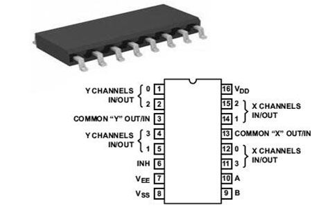
CD4052 Multiplexer Pinout

CD4052 Multiplexer Pinout


Pin   Number Pin Name Description
16 Vdd Positive power input,   maximum 20V
7 Vee Negative power rail,   normally connected to ground.
8 Vss (Ground) Connected to the ground   of the circuit
6 INH Enable pin – Must be   pulled to ground for normal operation
9,10 A,B Channel Select pins
1,12 Y0,X0 Channel 0 Input /   Output
5,14 Y1,X1 Channel 1 Input /   Output
2,15 Y2,X2 Channel 2 Input /   Output
4,11 Y3,X3 Channel 3 Input /   Output
3,13 Y,X Common Output / Input

CD4052 Multiplexer CAD Model

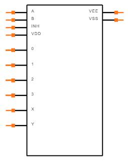
CD4052 Symbol

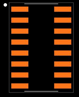
CD4052 Footprint

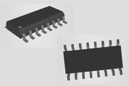
CD4052 3D Model

Specifications

CD4052BCM Tech Specifications

ON Semiconductor CD4052BCM technical specifications, attributes, parameters and parts with similar specifications to ON Semiconductor CD4052BCM.

Product Attribute Attribute Value
MountSurface Mount
Mounting TypeSurface Mount
Package / Case16-SOIC (0.154, 3.90mm Width)
Number of Pins16Pins
Supplier Device Package16-SOIC
Turn Off Delay Time420 ns
Operating Temperature-55°C~125°C TA
PackagingTube
Published2002
Part StatusObsolete
Moisture Sensitivity Level (MSL)1 (Unlimited)
Resistance1.05kOhm
Max Operating Temperature125°C
Min Operating Temperature-55°C
Max Power Dissipation500mW
Product Attribute Attribute Value
Base Part Number4052
Number of Outputs2Outputs
PolarityNon-Inverting
Number of Channels2Channels
Number of Circuits2Circuits
Max Supply Voltage15V
Min Supply Voltage5V
Nominal Supply Current20μA
Power Dissipation500mW
Throw ConfigurationSP4T
Propagation Delay55 ns
Turn On Delay Time1.2 μs
Logic FunctionDemultiplexer, Multiplexer
Number of Inputs8Inputs
Voltage - Supply, Single/Dual (±)5V~15V ±2.5V~7.5V
Product Attribute Attribute Value
Supply TypeDual, Single
Bandwidth40MHz
Max Dual Supply Voltage7.5V
Number of Gates2Gates
-3db Bandwidth40MHz
On-State Resistance (Max)240Ohm
Min Dual Supply Voltage2.5V
Multiplexer/Demultiplexer Circuit4:1
Current - Leakage (IS(off)) (Max)50nA
Switch CircuitSP4T
Switch Time (Ton, Toff) (Max)320ns, 150ns
Channel-to-Channel Matching (ΔRon)5Ohm
REACH SVHCUnknown
RoHS StatusRoHS Compliant
Lead FreeLead Free
0 Products View Similar

Features of CD4052 Multiplexer

  • Wide range of digital and analog signal levels: digital 3 – 15V, analog to 15Vp-p

  • Low “ON” resistance: 80Ω (typ.) over entire 15Vp-p signal-input range for VDD − VEE = 15V

  • High “OFF” resistance: channel leakage of ±10 pA (Typ.) at VDD − VEE = 10V

  • Logic level conversion for digital addressing signals of 3 – 15V (VDD − VSS = 3 – 15V) to switch analog signals to 15 Vp-p (VDD − VEE = 15V)

  • Matched switch characteristics: ∆RON = 5Ω (Typ.) for VDD − VEE = 15V

  • Very low quiescent power dissipation under all digital-control input and supply conditions: 1 µ W (typ.) at VDD − VSS = VDD − VEE = 10V

  • Binary address decoding on chip

CD4052 Multiplexer Equivalents

NTE4052, 4017

CD4052 Applications

  • Multiplexer and Demultiplexer circuit

  • A/D and D/A converter circuits

  • Network switching

  • Programmable Logic circuits

Where to Use CD4052

The CD4052 is a four-channel differential multiplexer/demultiplexer with two binary control inputs A and B. It accepts four inputs from four channels and outputs on channels X, Y, and an inhibit input in multiplexer mode. The two binary input signals A and B control which channels should be switched on.

The CD4052 IC can be used as a demultiplexer as well. It will only accept one input in this mode. The output will be routed to channel 0, 1, 2, or 3 depending on the selection pins A and B. Vss is connected to the circuit's ground, whereas Pin 15 is connected to the power supply. The inhibit pin is in charge of channel enabling and disabling. Channels are enabled when it is used with 0 logic. When the inhibit pin is applied with logic 1, no matter what input is applied on select pins, channels are disabled.


INH A B CHANNEL   SELECTION
LOW (0) 0 0 0
0 LOW 1 0 1
LOW 0 1 2
0 1 1 3
1 X X None

How to Use CD4052

Use CD4052 as a Multiplexer

It has two channels, X and Y, in multiplexer mode. X0 to X3 for channel X, and Y0 to Y3 for channel Y, are the four inputs for each channel. X and Y are the output pins for both channels. For both 4 cross 1 muxes, input pins A and B serve as common selection lines. These selection lines determine which input signal is shown on the output pin.

This is a working circuit diagram. We are getting output on X and Y pins according to the above table. You may also experiment with it with Proteus. As you can see, pins A and B on the selection line are equal to one. Multiplexer chooses X3 and Y3 inputs based on the selection lines. As a result, these inputs appear on output pins like X and Y.
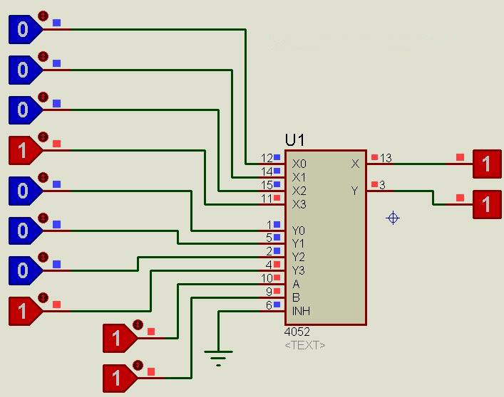
CD4052 Multiplexer Circuit


Use CD4052 as a Demux

This ic can also be used as a 14 multiplexer. It's also known as a decoder. X and Y are used as input pins in this setup. X0-X3 and Y0-Y3 on the other hand, use an output pin for X and Y, respectively. The selection pins A and B determine which pin output will be shown. As a result, based on digital logic on selected lines A and B, output pins will be X1, Y1 or X2, Y2 or X3, Y3 or X0, Y0.

The functioning principle of the demux is depicted in this simulation figure. As you can see in the figure, input X=1 and input Y=1 are both equal to zero, as are selection lines A and B. As a result, input signals appear on X0 and Y0. In other words, we can modify the values of the selection line signal to change the output.
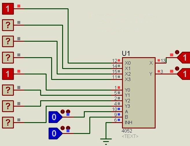
CD4052 Demux Circuit

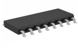
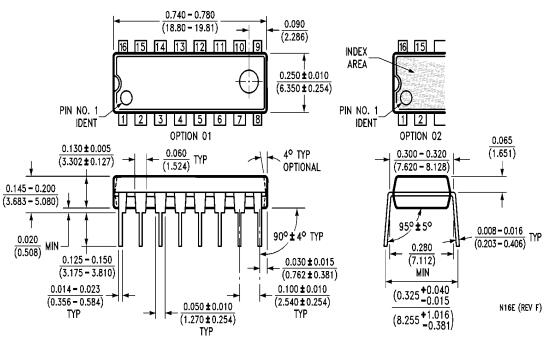
CD4052 Dimensions

CD4052 Dimensions

CD4052 Manufacturer

On Semiconductor (Nasdaq: ON) is a manufacturer engaging itself in reducing energy use. It features a comprehensive portfolio of power, signal management, and logic, custom solutions that are energy efficient. It acts as a world-class supply chain with high reliability and a network of manufacturing facilities, sales, offices, and design centers in key markets through North America, Europe, and the Asia Pacific regions.

Datasheet PDF

CD4052BCM Documents

Download datasheets and manufacturer documentation for CD4052BCM

Frequently Asked Questions

What is the use of CD4052?
CD4052 is a dual 4-channel IC that can be used as both a 4:1 multiplexer and 1:4 demultiplexer. It is a CMOS logic-based IC belonging to a CD4000 series of integrated circuits. We can use this IC in both digital and analog applications. In other words, it works for both analog and digital voltage levels.
How does CD4052 work?
CD4052 is a dual 4-channel differential multiplexer/demultiplexer IC with two binary control inputs A and B. Multiplexer mode takes 4 inputs from 4 channels and returns the output on channels X, Y. and an inhibit input.
What is the working principle of CD4052?
CD4052 is a differential 4-channel digitally controlled analog switch with two binary control inputs A and B and INH input. It has low on-resistance and a very low off-leakage current. A digital signal with an amplitude of 4.5-20V can control an analog signal with a peak-to-peak value of 20V.
What is the difference between CD4052 and CD4053?
4052----Dual 4 out of 1 analog switch. 4053----Three 2 out of 1 analog switch.
FAQ
What is the use of CD4052?
CD4052 is a dual 4-channel IC that can be used as both a 4:1 multiplexer and 1:4 demultiplexer. It is a CMOS logic-based IC belonging to a CD4000 series of integrated circuits. We can use this IC in both digital and analog applications. In other words, it works for both analog and digital voltage levels.
How does CD4052 work?
CD4052 is a dual 4-channel differential multiplexer/demultiplexer IC with two binary control inputs A and B. Multiplexer mode takes 4 inputs from 4 channels and returns the output on channels X, Y. and an inhibit input.
What is the working principle of CD4052?
CD4052 is a differential 4-channel digitally controlled analog switch with two binary control inputs A and B and INH input. It has low on-resistance and a very low off-leakage current. A digital signal with an amplitude of 4.5-20V can control an analog signal with a peak-to-peak value of 20V.
What is the difference between CD4052 and CD4053?
4052----Dual 4 out of 1 analog switch. 4053----Three 2 out of 1 analog switch.

TAGS

Share