ATTENTION: Due to increased demand and order volume, processing time may take an additional 1-3 business days.
HomeCommunitySubjectCD4066 Quad Bilateral Switches IC: Equivalent, Pinout and Use

CD4066 Quad Bilateral Switches IC: Equivalent, Pinout and Use

TEXAS INSTRUMENTS - CD4066BM - Analog Switch, Quad Channel, 4 Channels, SPST, 240 ohm, 3V to 18V, SOIC, 14 Pins

3675

Sep 2, 2021

Laurel Beerbohm

Audio Switch with CD4066


TEXAS INSTRUMENTS - CD4066BM - Analog Switch, Quad Channel, 4 Channels, SPST, 240 ohm, 3V to 18V, SOIC, 14 Pins

Hi, fellas. In today's new post, I will introduce CD4066 to you. CD4066 is a CMOS logic-based Quad Bilateral Switch IC belonging to a CD4000 family of integrated circuits. This article mainly introduces equivalent, pinout, uses, and other detailed information about Texas Instruments CD4066.
CD4066BM

30In Stock
Min.: 1 Mult.: 1
Quantity Unit Price Ext. Price
1+ $0.43259$0.43
10+ $0.4081$4.08
100+ $0.385$38.5
500+ $0.36321$181.61
1000+ $0.34265$342.65
Unit Price:$0.43259
Subtotal: $0.43
Looking for a better price? Want a lower wholesale price? Please send an RFQ, and we will respond immediately.
Quick Links

CD4066 Description

The CD4066 is a CMOS logic-based Quad Bilateral Switch IC belonging to a CD4000 family of integrated circuits. that is, It has four analog/digital switches which can be controlled individually using a control pin. 


These switches can conduct in both directions making it bilateral, it is commonly used for multiplexing analog or digital signals. Unlike the CD4016 IC, it provides low on-state resistance and resistance remains consistent for a full range of the input signal. 

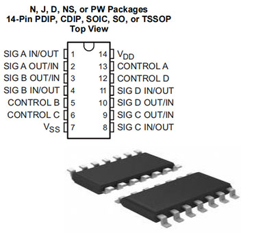
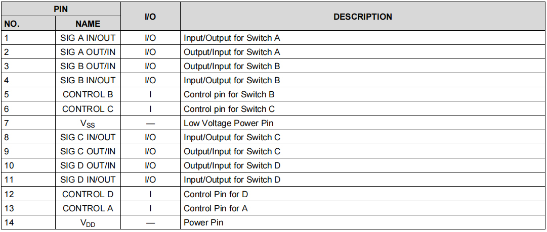
CD4066 Pinout

CD4066 CAD Model

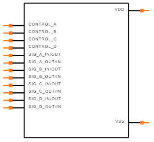
Symbol

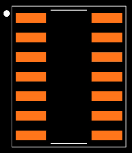
Footprint

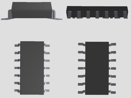
3D Model

CD4066 Features

-Quad Bilateral Switch for Multiplexing

-Very Low Internal Resistance

-Operating Voltage: 3V to 18V

-Switching Voltage: 20V (maximum)

-On-state Resistance: 5Ω (at 15V Vcc and 10kΩ Load)

-Output current High: -0.4mA

-Low Level Control pin Voltage: 0.9V (max)

-High Level Control pin Voltage: 11V (min @ 15V Vcc)

-Available in 14-pin PDIP, GDIP, PDSO packages

-Wide range of digital (15V) and Peak to Peak analog switching (±7.5 V)

-Noise immunity 0.45 VDD (Typ.)

-High Output-Voltage Ratio of 80 dB typically at fis = 10 kHz, RL = 1 kΩ

-Crosstalk between switches is –50 dB at fis = 8 MHz and RL = 1 kΩ which is very low


Specifications

Texas Instruments CD4066BM technical specifications, attributes, parameters and parts with similar specifications to Texas Instruments CD4066BM.

CD4066BM Tech Specifications

Texas Instruments CD4066BM technical specifications, attributes, parameters and parts with similar specifications to Texas Instruments CD4066BM.

Product Attribute Attribute Value
Lifecycle StatusACTIVE (Last Updated: 6 days ago)
Factory Lead Time6 Weeks
Contact PlatingGold
MountSurface Mount
Mounting TypeSurface Mount
Package / Case14-SOIC (0.154, 3.90mm Width)
Number of Pins14Pins
Weight129.387224mg
Turn Off Delay Time70 ns
Operating Temperature-55°C~125°C
PackagingTube
Series4000B
JESD-609 Codee4
Pbfree Codeyes
Part StatusActive
Moisture Sensitivity Level (MSL)1 (Unlimited)
Number of Terminations14Terminations
ECCN CodeEAR99
TypeBilateral, FET Switches
Product Attribute Attribute Value
Resistance1.05kOhm
Voltage - Supply3V~18V
Terminal FormGULL WING
Peak Reflow Temperature (Cel)260
Number of Functions4Functions
Supply Voltage5V
Terminal Pitch1.27mm
Base Part NumberCD4066
OutputSEPARATE OUTPUT
Pin Count14
Circuit1 x 1:1
PolarityNon-Inverting
Power Supplies5/15V
Number of Channels4Channels
Nominal Supply Current20nA
Max Supply Current5μA
Throw ConfigurationSPST
Quiescent Current20nA
Turn On Delay Time70 ns
Product Attribute Attribute Value
Supply TypeDual, Single
Neg Supply Voltage-Nom (Vsup)-5V
Max Dual Supply Voltage9V
Min Dual Supply Voltage1.5V
Dual Supply Voltage7.5V
Voltage Supply SourceDual Supply
On-state Resistance Match-Nom15Ohm
SwitchingBREAK-BEFORE-MAKE
Drain to Source Resistance240Ohm
Normal PositionNO
Signal Current-Max0.025A
Height1.75mm
Length8.65mm
Width3.91mm
Thickness1.58mm
REACH SVHCNo SVHC
Radiation HardeningNo
RoHS StatusROHS3 Compliant
Lead FreeLead Free
0 Products View Similar

CD4066 Alternatives

Part Number Description Manufacturer
5962R9665104VECSIGNAL CIRCUITS Single-Ended Multiplexer, 1 Func, 8 Channel, CMOS, CDIP16 Harris Semiconductor
MAX4051MJESIGNAL CIRCUITS Single-Ended Multiplexer, 1 Func, 8 Channel, CMOS, CDIP16, 0.300 INCH, CERAMIC, DIP-16 Maxim Integrated Products
CD4053BEXSIGNAL CIRCUITS IC,ANALOG MUX,TRIPLE,2-CHANNEL,CMOS,DIP,16PIN,PLASTIC Intersil Corporation
MC74HC4852ADTSIGNAL CIRCUITS Differential Multiplexer, 1 Func, 4 Channel, CMOS, PDSO16, PLASTIC, TSSOP-16 Motorola Semiconductor Products
MC74HC4053ADR2SIGNAL CIRCUITS TRIPLE 2-CHANNEL, SGL ENDED MULTIPLEXER, PDSO16, SOIC-16 Rochester Electronics LLC
CD74HC4052ESIGNAL CIRCUITS 5-V, 4:1 differential, 1-channel analog multiplexer 16-PDIP -55 to 125 Texas Instruments
MM74HC4066MSIGNAL CIRCUITS QUAD 1-CHANNEL, SGL POLE SGL THROW SWITCH, PDSO14 Texas Instruments
CD4051BD3SIGNAL CIRCUITS Single-Ended Multiplexer, 1 Func, 8 Channel, CMOS, CDIP16 Harris Semiconductor
MC74VHC4051DTR2GSIGNAL CIRCUITS Analog Multiplexer/ Demultiplexer, TSSOP-16, 2500-REEL ON Semiconductor
CD74HCT4053PWRLOGIC Multiplexer/Demultiplexer, Rochester Electronics LLC

Where to use CD4066?

The CD4066 is a bi-directional analog switching IC similar to CD4016, it is commonly used in multiplexing applications; it can also be used to isolate signals. The switch is bilateral and hence can be used for both digital and analog signals. The IC can operate from 3V to 18V but is commonly operated at 5V, 10Vor 15V nominal voltages. It can switch voltages up to 20V (peak).

How to use CD4066?

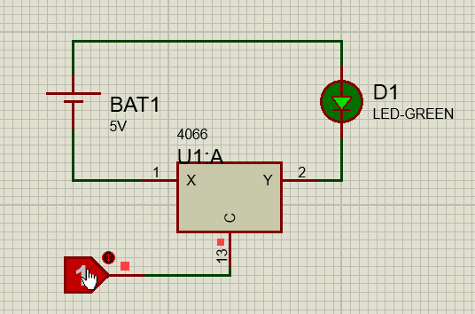
The CD4066 has four bilateral switches that can be controlled independently using a digital signal. Each switch has two input/output pins called SWx-IN and SWx-OUT. Both of which can be used as input or output pins, they can also be used to switch variable voltages like PWM wave, sine wave, etc of low magnitude and frequency. These two pins will be controlled by the control pin. The below simulation shows one out of the four switches in the IC.

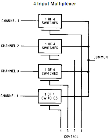
As you can see here the two switch pins are named X and Y and the control pin is named as C. By default when control pin is logic 0 (0V) the switch is open (not connected), but when a control signal is given to control pin C the switch closes and the LED glows. You can also use this IC as a 4-Input multiplexer by combining all the four switches to a common point as shown below.

CD4066 Applications

■Used in 4-Input Multiplexer

■ Used in the sample and Hold circuits

■ Used in network switching

■ Used in dead band filter

■ Used in switching and multiplexing of snalog signals and digital signals

■ Used in signal gating, modulators, demodulators, choppers, commutating Switches

■ Used in sogic Implementation of Transmission-Gates

■ Used in squelch control

■ Used in the conversion of analog-to-digital and digital-to-analog signals

■ Used in digital control of frequency, phase impedance, and analog-signal gain

■ Used in CMOS logic implementation


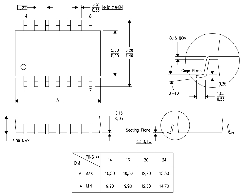
CD4066 Package

CD4066 Manufacturer

Texas Instruments (TI) is an American technology company headquartered in Dallas, Texas, which designs and manufactures semiconductors and various integrated circuits, and sells them to electronic designers and manufacturers worldwide. It is one of the top 10 semiconductor companies in global sales. The company focuses on the development of analog chips and embedded processors, which account for more than 80% of its revenue. TI also produces TI digital light processing technology and educational technology products, including calculators, microcontrollers and multi-core processors. As of 2016, the company has 45,000 patents worldwide.

Datasheet PDF

Download datasheets and manufacturer documentation for Texas Instruments CD4066BM.

CD4066BM Documents

Download datasheets and manufacturer documentation for CD4066BM

Frequently Asked Questions

1.When is the input voltage of CD4066 turned on?
The control signal level of CD4066 varies with the operating voltage: when CD4066 is working under 5V voltage, the high level is 3.5V, the low level is 1V, and when the control signal is higher than 3.5V, ensure that the corresponding channel is turned on When the control signal is lower than 1V, ensure that the corresponding channel is turned off; when the CD4066 is working at 15V, the high level is 11V, the low level is 2V, and when the control signal is higher than 11V, ensure that the corresponding channel is turned on When the control signal is lower than 2V, ensure that the corresponding channel is turned off. From this estimate, the high-level threshold is approximately equivalent to 0.7 times the power supply voltage.
2.What is the working principle of CD4066?
CD4066 is a two-way analog switch. There are 4 independent analog switches in the integrated circuit that can control the transmission of digital and analog signals. Each switch has an input terminal and an output terminal, they can be used interchangeably, and there is a strobe terminal (also called control terminal), when the strobe terminal is high, the switch is turned on; when the strobe terminal is low power Usually, the switch is off. When in use, the strobe terminal is not allowed to be left floating.
3.CD4066 application circuit VDD is positive or negative?
VDD is positive plus positive voltage.
FAQ
1.When is the input voltage of CD4066 turned on?
The control signal level of CD4066 varies with the operating voltage: when CD4066 is working under 5V voltage, the high level is 3.5V, the low level is 1V, and when the control signal is higher than 3.5V, ensure that the corresponding channel is turned on When the control signal is lower than 1V, ensure that the corresponding channel is turned off; when the CD4066 is working at 15V, the high level is 11V, the low level is 2V, and when the control signal is higher than 11V, ensure that the corresponding channel is turned on When the control signal is lower than 2V, ensure that the corresponding channel is turned off. From this estimate, the high-level threshold is approximately equivalent to 0.7 times the power supply voltage.
2.What is the working principle of CD4066?
CD4066 is a two-way analog switch. There are 4 independent analog switches in the integrated circuit that can control the transmission of digital and analog signals. Each switch has an input terminal and an output terminal, they can be used interchangeably, and there is a strobe terminal (also called control terminal), when the strobe terminal is high, the switch is turned on; when the strobe terminal is low power Usually, the switch is off. When in use, the strobe terminal is not allowed to be left floating.
3.CD4066 application circuit VDD is positive or negative?
VDD is positive plus positive voltage.

TAGS

Share