ATTENTION: Due to increased demand and order volume, processing time may take an additional 1-3 business days.
HomeCommunitySubjectCD4066B Bilateral Switch: Features, Speicifications and Applications

CD4066B Bilateral Switch: Features, Speicifications and Applications

Switch, Bilateral; PDIP; Quad Bilateral Switch Logic; 18 (max.)v; -55; +125 The CD4066B device is a quad bilateral switch intended for the transmission or multiplexing of analog or digital signals.

163

Mar 19, 2021

Polly

Switch, Bilateral; PDIP; Quad Bilateral Switch Logic; 18 (max.)v; -55; 125

The CD4066B device is a quad bilateral switch intended for the transmission or multiplexing of analog or digital signals. It is pin-for-pin compatible with the CD4016B device, but exhibits a much lower on-state resistance. In addition, the on-state resistance is relatively constant over the full signalinput range.

CD4066BE

5000In Stock
Min.: 1 Mult.: 1
Quantity Unit Price Ext. Price
1+ $0.75194$0.75
10+ $0.70938$7.09
100+ $0.66923$66.92
500+ $0.63135$315.68
1000+ $0.59561$595.61
Unit Price:$0.75194
Subtotal: $0.75
Looking for a better price? Want a lower wholesale price? Please send an RFQ, and we will respond immediately.
Quick Links

CD4066B Description

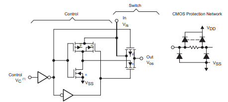
The CD4066B device is a quad bilateral switch intended for the transmission or multiplexing of analog or digital signals. It is pin-for-pin compatible with the CD4016B device, but exhibits a much lower on-state resistance. In addition, the on-state resistance is relatively constant over the full signalinput range. The CD4066B device consists of four bilateral switches, each with independent controls. Both the p and the n devices in a given switch are biased on or off simultaneously by the control signal. As shown in Figure below, the well of the n-channel device on each switch is tied to either the input (when the switch is on) or to VSS (when the switch is off). This configuration eliminates the variation of the switchtransistor threshold voltage with input signal and, thus, keeps the on-state resistance low over the full operating-signal range. The advantages over single-channel switches include peak input-signal voltage swings equal to the full supply voltage and more constant on-state impedance over the input-signal range. However, for sample-and-hold applications, the CD4016B device is recommended.

CD4066B Features

• 15-V Digital or ±7.5-V Peak-to-Peak Switching 

• 125-Ω Typical On-State Resistance for 15-V Operation 

• Switch On-State Resistance Matched to Within 5 Ω Over 15-V Signal-Input Range 

• On-State Resistance Flat Over Full Peak-to-Peak Signal Range 

• High On or Off Output-Voltage Ratio: 80 dB Typical at fis = 10 kHz, RL = 1 kΩ 

• High Degree of Linearity: <0.5% Distortion Typical at fis = 1 kHz, Vis = 5-Vp-p VDD – VSS ≥ 10-V, RL = 10 kΩ 

• Extremely Low Off-State Switch Leakage, Resulting in Very Low Offset Current and High Effective Off-State Resistance: 10 pA Typical at VDD – VSS = 10-V, TA = 25°C 

• Extremely High Control Input Impedance (Control Circuit Isolated From Signal Circuit): 1012 Ω Typical 

• Low Crosstalk Between Switches: –50 dB Typical at fis = 8 MHz, RL = 1 kΩ 

• Matched Control-Input to Signal-Output Capacitance: Reduces Output Signal Transients 

• Frequency Response, Switch On = 40 MHz Typical 

• 100% Tested for Quiescent Current at 20-V 

• 5-V, 10-V, and 15-V Parametric Ratings

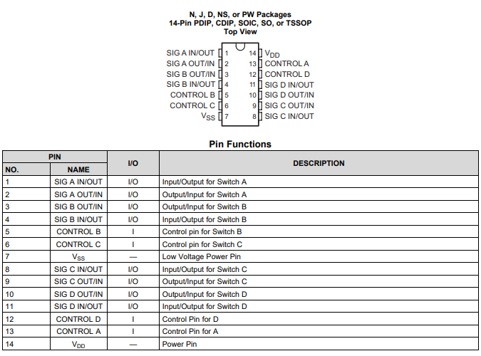
CD4066B Pins

Specifications

Texas Instruments CD4066BE technical specifications, attributes, parameters and parts with similar specifications to Texas Instruments CD4066BE.

CD4066BE Tech Specifications

Texas Instruments CD4066BE technical specifications, attributes, parameters and parts with similar specifications to Texas Instruments CD4066BE.

Product Attribute Attribute Value
Lifecycle StatusACTIVE (Last Updated: 1 day ago)
Factory Lead Time6 Weeks
Contact PlatingGold
MountThrough Hole
Mounting TypeThrough Hole
Package / Case14-DIP (0.300, 7.62mm)
Number of Pins14Pins
Weight927.99329mg
Turn Off Delay Time30 ns
Operating Temperature-55°C~125°C
PackagingTube
Series4000B
JESD-609 Codee3
Part StatusActive
Moisture Sensitivity Level (MSL)1 (Unlimited)
Number of Terminations14Terminations
ECCN CodeEAR99
TypeBilateral, FET Switches
Resistance240Ohm
Terminal FinishMatte Tin (Sn)
Product Attribute Attribute Value
Voltage - Supply3V~18V
Number of Functions4Functions
Supply Voltage5V
Frequency40MHz
Base Part NumberCD4066
Pin Count14
Number of Outputs2Outputs
Circuit1 x 1:1
PolarityNon-Inverting
Power Supplies5/15V
Number of Channels4Channels
Max Supply Current5μA
Throw ConfigurationSPST
Quiescent Current20nA
Turn On Delay Time30 ns
Number of Inputs3Inputs
Supply TypeDual, Single
Bandwidth40MHz
Neg Supply Voltage-Nom (Vsup)-5V
Max Dual Supply Voltage9V
Product Attribute Attribute Value
Min Dual Supply Voltage1.5V
Dual Supply Voltage7.5V
Input Capacitance8pF
Voltage Supply SourceDual Supply
On-state Resistance Match-Nom15Ohm
SwitchingBREAK-BEFORE-MAKE
Switch-on Time-Max70ns
Switch-off Time-Max70ns
Drain to Source Resistance470Ohm
Normal PositionNO
Ambient Temperature Range High125°C
Height5.08mm
Length19.3mm
Width6.35mm
Thickness3.9mm
REACH SVHCNo SVHC
Radiation HardeningNo
RoHS StatusROHS3 Compliant
Lead FreeLead Free
0 Products View Similar

CD4066B Applications

• Analog Signal Switching and Multiplexing: Signal Gating, Modulators, Squelch Controls, Demodulators, Choppers, Commutating Switches 

• Digital Signal Switching and Multiplexing 

• Transmission-Gate Logic Implementation 

• Analog-to-Digital and Digital-to-Analog Conversions 

• Digital Control of Frequency, Impedance, Phase, and Analog-Signal Gain 

• Building Automation

Datasheet PDF

Download datasheets and manufacturer documentation for Texas Instruments CD4066BE.

CD4066BE Documents

Download datasheets and manufacturer documentation for CD4066BE

Frequently Asked Questions

How does a bilateral switch work?
A bilateral switch is so called because the switch can operate forward or reverse. This means that either side of the switch can be used as the input. So current can flow in one direction and the other direction, depending on which side is the input. A bilateral switch acts as a single pole, single throw switch.
FAQ
How does a bilateral switch work?
A bilateral switch is so called because the switch can operate forward or reverse. This means that either side of the switch can be used as the input. So current can flow in one direction and the other direction, depending on which side is the input. A bilateral switch acts as a single pole, single throw switch.

TAGS

Share