ATTENTION: Due to increased demand and order volume, processing time may take an additional 1-3 business days.
HomeCommunitySubjectCD4069 Inverter CMOS: Pinout, Datasheet pdf and Circuit

CD4069 Inverter CMOS: Pinout, Datasheet pdf and Circuit

Logic - Gates and Inverters 14-DIP (0.300, 7.62mm) 3V~15V -55°C~125°C 4000B 4069 FAIRCHILD SEMICONDUCTOR CD4069UBCN4000 CMOS (MM74C04N), 4069, DIP14

13981

Oct 31, 2021

Riva Marshall

Chip-Chat #1 - CMOS CD 4069 Inverter - Ec-Projects

Logic - Gates and Inverters 14-DIP (0.300, 7.62mm) 3V~15V -55°C~125°C 4000B 4069 FAIRCHILD SEMICONDUCTOR CD4069UBCN4000 CMOS (MM74C04N), 4069, DIP14

The CD4069 is made up of six inverter circuits and is made with complementary MOS (CMOS) technology to produce a wide operating range, low power consumption, good noise immunity, and symmetric controlled rise and fall timings. This article is going to explain datasheet pdf, pinout, applications, circuit, equivalents, and other details about CD4069 Inverter CMOS.

CD4069UBCN

6050In Stock
Min.: 1 Mult.: 1
Price not displayed? Not available to buy online? Please send an RFQ, and we will respond immediately.
Quick Links

What is CD4069 Inverter?

The CD4069 is made up of six inverter circuits and is made with complementary MOS (CMOS) technology to produce a wide operating range, low power consumption, good noise immunity, and symmetric controlled rise and fall timings.

This device is designed for all general-purpose inverter applications that do not require the specific features of the MM74C901, MM74C907, or CD4049A Hex Inverter/Buffers. The MM74C14 or MM74C914 Hex Schmitt Trigger is recommended for situations requiring higher noise immunity.

Diode clamps to VDD and VSS safeguard all inputs from harm caused by static discharge.

CD4069 Inverter Pinout

CD4069 Inverter Pinout


Pin No Pin Name Description
1 A the input of inverter A
2 A’ the inverted output of A
3 B the input of inverter B
4 B’ the inverted output of B
5 C the input of inverter C
6 C’ the inverted output of C
7 VSS source supply
8 D’ the inverted output of D
9 D the input of inverter D
10 E’ the inverted output of E
11 E the input of inverter E
12 F’ the inverted output of F
13 F the input of inverter F
14 VDD Drain supply

CD4069 Inverter CAD Model

CD4069 Inverter Symbol

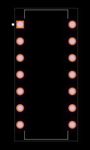
CD4069 Inverter Footprint

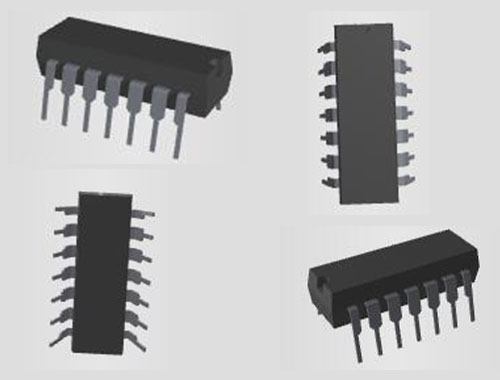
CD4069 Inverter 3D Model

Specifications

CD4069UBCN Tech Specifications

ON Semiconductor CD4069UBCN technical specifications, attributes, parameters and parts with similar specifications to ON Semiconductor CD4069UBCN.

Product Attribute Attribute Value
MountThrough Hole
Mounting TypeThrough Hole
Package / Case14-DIP (0.300, 7.62mm)
Number of Pins14Pins
Supplier Device Package14-PDIP
Logic Level-High4V ~ 12V
Logic Level-Low1V ~ 3V
Number of Elements6 Elements
Operating Temperature-55°C~125°C
PackagingTube
Series4000B
Published2002
Part StatusObsolete
Product Attribute Attribute Value
Moisture Sensitivity Level (MSL)1 (Unlimited)
Max Operating Temperature125°C
Min Operating Temperature-55°C
Voltage - Supply3V~15V
Base Part Number4069
Voltage15V
Number of Circuits6Circuits
Max Supply Voltage15V
Min Supply Voltage3V
Output Current8.8mA
Propagation Delay50 ns
Quiescent Current1μA
Turn On Delay Time90 ns
Product Attribute Attribute Value
Logic FunctionBuffer, Inverter
Number of Inputs6Inputs
Logic TypeInverter
Number of Gates6Gates
Max Propagation Delay @ V, Max CL50ns @ 15V, 50pF
High Level Output Current-4.2mA
Low Level Output Current4.2mA
Current - Quiescent (Max)1μA
REACH SVHCNo SVHC
Radiation HardeningNo
RoHS StatusRoHS Compliant
Lead FreeLead Free
0 Products View Similar

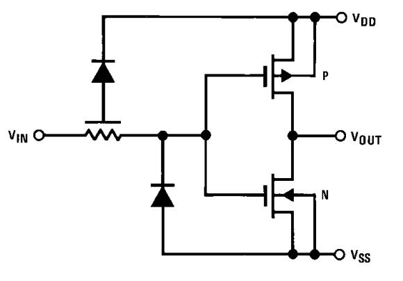
CD4069 Inverter Schematics Diagram

From the CD4069 Inverter schematic diagram, it is clear that it is made up of MOSFET N and P structures.

It provides excellent Inverter gate logic according to CMOS principles. That is both low-energy and high-quality.

CD4069 Inverter Schematics Diagram

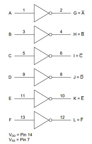
CD4069 Inverter Functional Block Diagram

CD4069 Inverter Functional Block Diagram

CD4069 Inverter Features

  • Wide supply voltage range: 3.0V to 15V

  • High noise immunity: 0.45 VDD type.

  • Low power TTL compatibility: Fan out of 2 driving 74L or 1 driving 74LS

  • Equivalent to MM74C04

CD4069 Inverter Equivalents

MC14069, TC14069, HD14069, MM74C04

CD4069 Inverter Applications

  • Logic inversion

  • Pulse shaping

  • Oscillators

  • High-input-impedance amplifiers

CD4069 Inverter Circuit

CD4069 Inverter 1 kHz Clock pulse generator

The output is a square wave frequency or pulse form. And F = 1 / 1.4 RC.

CD4069 Inverter Bounceless Switch circuit

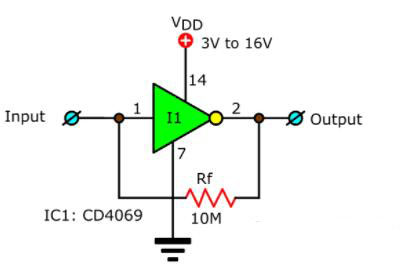
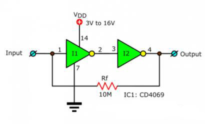
CD4069 Inverter High-Input Impedance Amplifier

If your input signals aren't strong enough. It may cause a circuit malfunction. Before a feed to the circuit, we need to increase it. As a high-impedance amplifier, an Inverter or buffer gate is a simple solution.

We'll see a power amplifier with a digital logic gate later.

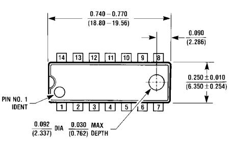
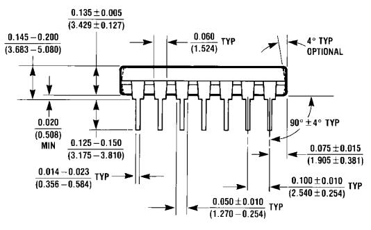
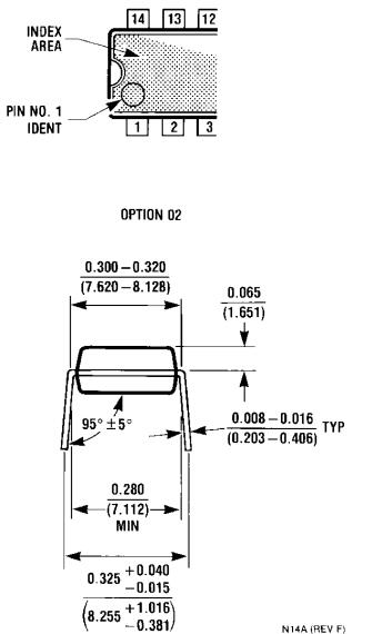
CD4069 Inverter Dimensions

CD4069 Inverter Dimensions

CD4069 Inverter Manufacturer

On Semiconductor (Nasdaq: ON) is a manufacturer engaging itself in reducing energy use. It features a comprehensive portfolio of power, signal management, and logic, custom solutions that are energy efficient. It acts as a world-class supply chain with high reliability and a network of manufacturing facilities, sales, offices, and design centers in key markets through North America, Europe, and the Asia Pacific regions.

Datasheet PDF

CD4069UBCN Documents

Download datasheets and manufacturer documentation for CD4069UBCN

Frequently Asked Questions

What is CD4069 used for?
The CD4069 device consists of six CMOS inverter circuits. These devices are intended for all general-purpose inverter applications where the medium-power TTL-drive and logic-level-conversion capabilities of circuits such as the CD4009 and CD4049 hex inverter and buffers are not required.
How does CD4069 work?
As the voltage increases from zero, the first LED grows in brightness. Just when that LED is fully lit, the next LED begins to glow slightly. Each LED represents about 1 volt of change when the circuit is operating from 9 volts.
How many NOT gates are on the 4069?
You use the C-MOS IC 4069, which has six NOT gates. The circuit shown is therefore only one example, since you can use any of the six gates.
What is CMOS inverter?
A CMOS inverter is a field-effect transistor that is composed of a metal gate that lies on top of an insulating layer of oxygen, which lies on top of a semiconductor. CMOS inverters are found in most electronic devices and are responsible for producing data within small circuits.
What is the voltage of CD4069?
3.0V to 15V
FAQ
What is CD4069 used for?
The CD4069 device consists of six CMOS inverter circuits. These devices are intended for all general-purpose inverter applications where the medium-power TTL-drive and logic-level-conversion capabilities of circuits such as the CD4009 and CD4049 hex inverter and buffers are not required.
How does CD4069 work?
As the voltage increases from zero, the first LED grows in brightness. Just when that LED is fully lit, the next LED begins to glow slightly. Each LED represents about 1 volt of change when the circuit is operating from 9 volts.
How many NOT gates are on the 4069?
You use the C-MOS IC 4069, which has six NOT gates. The circuit shown is therefore only one example, since you can use any of the six gates.
What is CMOS inverter?
A CMOS inverter is a field-effect transistor that is composed of a metal gate that lies on top of an insulating layer of oxygen, which lies on top of a semiconductor. CMOS inverters are found in most electronic devices and are responsible for producing data within small circuits.
What is the voltage of CD4069?
3.0V to 15V

TAGS

Share