ATTENTION: Due to increased demand and order volume, processing time may take an additional 1-3 business days.
HomeCommunitySubjectCD4081 Quad 2 Input AND Gate IC: Pinout, Datasheet and Circuit

CD4081 Quad 2 Input AND Gate IC: Pinout, Datasheet and Circuit

IC, 4000 CMOS, 4081, DIP14, 18V The CD4081 is a four-AND gate CMOS chip. This article mainly covers pinout, circuit, datasheet, features, and more details about CD4081 gate IC. Furthermore, there is a huge range of semiconductors, capacitors, resistors, and ICs in stock. Welcome your RFQ!

6524

Oct 3, 2021

Alva Kelsen


CD4081 | AND gate IC 4081 with truth table | Two input AND gate


IC, 4000 CMOS, 4081, DIP14, 18V

The CD4081 is a four-AND gate CMOS chip. This article mainly covers pinout, circuit, datasheet, features, and more details about CD4081 gate IC. Furthermore, there is a huge range of semiconductors, capacitors, resistors, and ICs in stock. Welcome your RFQ!

CD4081BE

5In Stock
Min.: 1 Mult.: 1
Quantity Unit Price Ext. Price
1+ $1.52218$1.52
10+ $1.43602$14.36
100+ $1.35474$135.47
500+ $1.27805$639.03
1000+ $1.20571$1205.71
Unit Price:$1.52218
Subtotal: $1.52
Looking for a better price? Want a lower wholesale price? Please send an RFQ, and we will respond immediately.
Quick Links

What is CD4081?

The CD4081 is a four-AND gate CMOS chip. An AND gate is a logic gate that only outputs a HIGH value when all of its inputs are also HIGH. There are four AND gates in this Integrated Circuit (IC), each with two inputs. As a result, it's commonly referred to as a Quad 2-Input AND Gate.

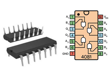
CD4081 Pinout

CD4081 Pinout


Pin   Number Pin Name Pin Description
14 VDD Supply voltage input,   5V to 15V
7 VSS Ground reference
1, 2 INPUT AND gate one input
3 OUTPUT AND gate one output
5, 6 INPUT AND gate two inputs
4 OUTPUT AND gate two output
8, 9 INPUT AND gate three inputs
10 OUTPUT AND gate three output
12, 13 INPUT AND gate four inputs
11 OUTPUT AND gate four output

CD4081 CAD Model

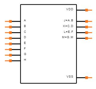
CD4081 Symbol


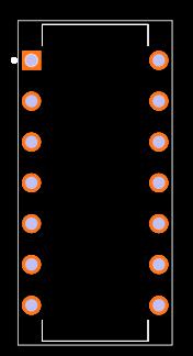
CD4081 Footprint


CD4081 3D Model


CD4081 Features

  • Four two-input AND gates in one package

  • Wide supply range – 5V to 15V typical

  • 700mW power dissipation

  • Symmetrical output characteristics

  • Maximum input leakage 1 µA at 15V over a full temperature range

  • Available in DIP-14 package

Specifications

CD4081BE Tech Specifications

Texas Instruments CD4081BE technical specifications, attributes, parameters and parts with similar specifications to Texas Instruments CD4081BE.

Product Attribute Attribute Value
Lifecycle StatusACTIVE (Last Updated: 2 days ago)
Factory Lead Time12 Weeks
Contact PlatingGold
MountThrough Hole
Mounting TypeThrough Hole
Package / Case14-DIP (0.300, 7.62mm)
Number of Pins14Pins
Weight927.99329mg
Logic Level-High3.5V ~ 11V
Logic Level-Low1.5V ~ 4V
Number of Elements4 Elements
Operating Temperature-55°C~125°C
PackagingTube
Series4000B
JESD-609 Codee4
Part StatusActive
Moisture Sensitivity Level (MSL)1 (Unlimited)
Product Attribute Attribute Value
Number of Terminations14Terminations
TerminationThrough Hole
ECCN CodeEAR99
Voltage - Supply3V~18V
Terminal PositionDUAL
Number of Functions4Functions
Supply Voltage5V
Base Part NumberCD4081
Pin Count14
Number of Outputs1Output
Max Output Current6.8mA
Supply Voltage-Min (Vsup)3V
Load Capacitance50pF
Power Dissipation100mW
Output Current6.8mA
Propagation Delay90 ns
Quiescent Current5μA
Product Attribute Attribute Value
Turn On Delay Time90 ns
Logic FunctionAND
Number of Inputs2Inputs
Logic TypeAND Gate
Max I(ol)0.0068 A
Max Propagation Delay @ V, Max CL90ns @ 15V, 50pF
Input Capacitance5pF
Current - Quiescent (Max)1μA
Schmitt Trigger InputNo
Height5.08mm
Length19.3mm
Width6.35mm
Thickness3.9mm
REACH SVHCNo SVHC
RoHS StatusROHS3 Compliant
Lead FreeLead Free
0 Products View Similar

CD4081 Applications

  • Logic buffers, inverters, and decoders

  • Implementing logic circuits

  • Signal conditioning

  • Enable gate

  • Inhibit gate

  • Measurement of frequency

Alternatives for CD4081

NTE4081, MC14081, HCF4081, TC4081, HEF4081, 74HC08, 74HC09, 74HC131, 74HC09, CD4071, CD4013, CD4017, CD4045, CD4019 

How to Use CD4081

To use any of the OR gates in the chip, you must first connect the power supply to the VDD and GND pins. You'll need a power supply with a voltage ranging from 3 to 15 volts.

Some variants of the chip can withstand up to 20 volts. For accurate values, consult the datasheet for your chip's version.

The four AND gates in the IC are fed by the A and B pins. The outcome is determined by what you enter here.

The AND gates' outputs are represented by the Q pins.

CD4081 Circuit

Here's an example of a circuit you can make with a CD4081 chip.

The circuit explains how an AND gate works in its most basic form. This is a great project to learn how an AND gate works.

Both inputs to the AND gate are normally LOW. To view what the AND gate outputs, press any of the pushbuttons to establish a HIGH on either input pin. A brightly lighted LED denotes a high output. A LOW output is represented by an unlit LED.


Component Required

  • Two pushbuttons

  • A Red LED

  • Three 10 kΩ resistors

  • A chip with AND gates such as the CD4081

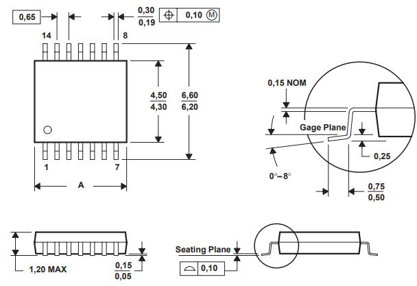
CD4081 Dimension

CD4081 Dimension

CD4081 Manufacturer

Texas Instruments (TI) emerges as a globally recognized semiconductor manufacturer expanded into 35 countries. It has seen rapid growth. In 1958, TIer firstly introduced the working integrated circuit. And today more than 30,000 TIers worldwide are committed to designing, manufacturing, and selling analog and embedded processing chips. They aspire to solve challenges as well as change the world through their technologies.

Datasheet PDF

Download datasheets and manufacturer documentation for Texas Instruments CD4081BE.

CD4081BE Documents

Download datasheets and manufacturer documentation for CD4081BE

Frequently Asked Questions

How does CD4081 work?
The CD4081 AND gate is a basic digital logic gate that implements logical conjunction (∧) from mathematical logic – it behaves according to the truth table above. A HIGH output (1) results only if all the inputs to the AND gate are HIGH (1). If none or not all inputs to the AND gate are HIGH, LOW output results.
What is the logical symbol of cd4081?
Cd4081 is four 2-input AND gates, two 2-input AND gate logic symbols.
FAQ
How does CD4081 work?
The CD4081 AND gate is a basic digital logic gate that implements logical conjunction (∧) from mathematical logic – it behaves according to the truth table above. A HIGH output (1) results only if all the inputs to the AND gate are HIGH (1). If none or not all inputs to the AND gate are HIGH, LOW output results.
What is the logical symbol of cd4081?
Cd4081 is four 2-input AND gates, two 2-input AND gate logic symbols.

TAGS

Share