ATTENTION: Due to increased demand and order volume, processing time may take an additional 1-3 business days.
HomeCommunitySubjectCD4503 Tri-state Hex Buffer: CD4503 Datasheet PDF, Pinout, CD4503 vs. MC14503

CD4503 Tri-state Hex Buffer: CD4503 Datasheet PDF, Pinout, CD4503 vs. MC14503

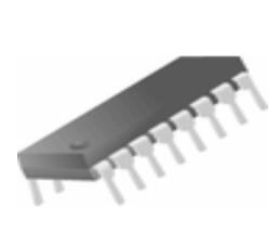
Logic - Buffers, Drivers, Receivers, Transceivers DIP 5V ONE FUNCTION WITH TWO BITS BUS DRIVER CD4503 is a hex non-inverting buffer with 3-state outputs having high sink- and source-current capability.

809

Dec 2, 2021

Berg Rossetti

Logic - Buffers, Drivers, Receivers, Transceivers DIP 5V ONE FUNCTION WITH TWO BITS BUS DRIVER

CD4503 is a hex non-inverting buffer with 3-state outputs having high sink- and source-current capability. This article will cover its datasheet, pinout, feature and more details about CD4503. Welcome your RFQ!
CD4503BCN

Inquiry
Min.: 1 Mult.: 1
Price not displayed? Not available to buy online? Please send an RFQ, and we will respond immediately.
Quick Links

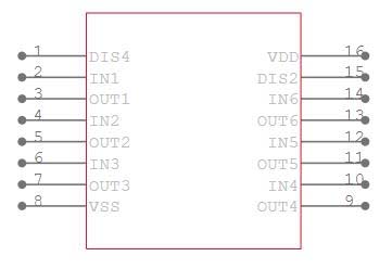
CD4503 Pinout

CD4503 Pinout


Pin No

Pin Name

Description

1

DIS A

Disable A

2

D1

Input Pin Buffer 1

3

Q1

Output Pin Buffer 1

4

D2

Input Pin Buffer 2

5

Q2

Output Pin Buffer 2

6

D3

Input Pin Buffer 3

7

Q3

Output Pin Buffer 3

8

VSS

Source Supply

9

Q4

Output Pin Buffer 4

10

D4

Input Pin Buffer 4

11

Q5

Output Pin Buffer 5

12

D5

Input Pin Buffer 5

13

Q6

Output Pin Buffer 6

14

D6

Input Pin Buffer 6

15

DIS B

Disable B

16

VDD

Drain supply

CD4503 CAD Model

CD4503 Symbol


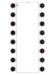
CD4503 Footprint


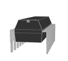
CD4503 3D Model

CD4503 Descripton

CD4503 is a hex non-inverting buffer with three-state outputs that can handle a lot of sinks and source current. In 16-lead hermetic dual-in-line ceramic packaging, the CD4503 Hex buffer is available. This  IC  family offers a variety of functions, including ESD protection and thermal overload protection. In DLD design and logic switching applications, the Hex Buffer CD4503 is critical.

CD4503 Feature

■ Wide supply voltage range: 3.0 VDC to 18 VDC

■ 3-STATE outputs 

■ Symmetrical turn on/turn off delays 

■ Symmetrical output rise and fall times 

■ Pin-for-pin replacement for MM80C97 and MC14503

CD4503 Application

  • 3-State hex buffer for interfacing IC'S with data buses

  • CMOS to TTL Hex Buffer

  • Hex Buffers are also used to isolate other gates or circuit stages from each other preventing the impedance of one circuit from affecting the impedance of another


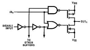
CD4503 Schematic

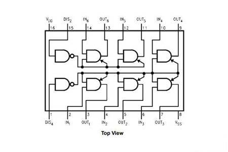
The following figure shows a schematic diagram of CD4503:

CD4503 Schematic Diagram

Specifications

Fairchild (ON Semiconductor) CD4503BCN technical specifications, attributes, parameters and parts with similar specifications to Fairchild (ON Semiconductor) CD4503BCN.

CD4503BCN Tech Specifications

ON Semiconductor CD4503BCN technical specifications, attributes, parameters and parts with similar specifications to ON Semiconductor CD4503BCN.

Product Attribute Attribute Value
Mounting TypeThrough Hole
Package / Case16-DIP (0.300, 7.62mm)
Supplier Device Package16-PDIP
Number of Elements2 Elements
Operating Temperature-55°C~125°C TA
Product Attribute Attribute Value
PackagingTube
Series4000B
Published2004
Part StatusObsolete
Moisture Sensitivity Level (MSL)1 (Unlimited)
Product Attribute Attribute Value
Voltage - Supply3V~15V
Base Part Number4503
Output TypePush-Pull
Logic TypeBuffer, Non-Inverting
Number of Bits per Element2, 4 (Hex)
0 Products View Similar

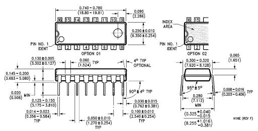
CD4503 Physical Dimensions

CD4503 Physical Dimensions

CD4503 Manufacturer

ON Semiconductor has completed its acquisition of Fairchild. Together, we deliver a more extensive product portfolio of power discretes, ICs and power modules, plus a complete offering of low, mid and high voltage products across the entire voltage spectrum which means more choices for your designs. Together, we provide a stronger presence in the key markets of automotive, industrial and wireless, combined with increased technical and sales support.

Datasheet PDF

CD4503BCN Documents

Download datasheets and manufacturer documentation for CD4503BCN

Frequently Asked Questions

What is A Hex Buffer?
A buffer is a simple logic gate that sends its input to its output unmodified. It behaves in the opposite way that a NOT gate does. The primary function of a buffer is to regenerate the input signal, which is commonly accomplished by utilizing a strong high and a strong low. A buffer has only one input and output, and its output is always the same as its input. Buffers are also utilized to drive huge capacitive loads, which increases the propagation delay of circuits.
What is a hex buffer used for?
These hex buffers and drivers feature high-voltage open-collector outputs to interface with high-level circuits or for driving high-current loads. They are also characterized for use as buffers for driving TTL inputs.
What is the difference between buffer and inverter?
An inverter is a logic gate whose output (X) is the inverse of its input (A). A buffer is a type of logic gate that is used to increase drive capability in order to increase the number of fanouts or the signal speed. A buffer does not perform any logical operation. It also helps shape the waveform of a signal.
FAQ
What is A Hex Buffer?
A buffer is a simple logic gate that sends its input to its output unmodified. It behaves in the opposite way that a NOT gate does. The primary function of a buffer is to regenerate the input signal, which is commonly accomplished by utilizing a strong high and a strong low. A buffer has only one input and output, and its output is always the same as its input. Buffers are also utilized to drive huge capacitive loads, which increases the propagation delay of circuits.
What is a hex buffer used for?
These hex buffers and drivers feature high-voltage open-collector outputs to interface with high-level circuits or for driving high-current loads. They are also characterized for use as buffers for driving TTL inputs.
What is the difference between buffer and inverter?
An inverter is a logic gate whose output (X) is the inverse of its input (A). A buffer is a type of logic gate that is used to increase drive capability in order to increase the number of fanouts or the signal speed. A buffer does not perform any logical operation. It also helps shape the waveform of a signal.

TAGS

Share