ATTENTION: Due to increased demand and order volume, processing time may take an additional 1-3 business days.
HomeCommunitySubjectCY7C4255V Low Voltage Deep Sync FIFOs: Pinout, Equivalent and Datasheet

CY7C4255V Low Voltage Deep Sync FIFOs: Pinout, Equivalent and Datasheet

IC DEEP SYNC FIFO 8KX18 64LQFP The CY7C4255V is high speed, low power, first-in first-out (FIFO) memory with clocked read and write interfaces. It is 18 bits wide and is pin and functionally compatible to the CY7C42X5V Synchronous FIFO family.

123

Apr 18, 2022

Hilary Russell

Synchronous FIFO / FIFO-part ll


IC DEEP SYNC FIFO 8KX18 64LQFP

The CY7C4255V is high speed, low power, first-in first-out (FIFO) memory with clocked read and write interfaces. It is 18 bits wide and is pin and functionally compatible to the CY7C42X5V Synchronous FIFO family. The CY7C4255V can be cascaded to increase FIFO depth. Furthermore, Huge range of Semiconductors, Capacitors, Resistors and IcS in stock. Welcome RFQ.
CY7C4255V-15ASXC

49In Stock
Min.: 1 Mult.: 1
Quantity Unit Price Ext. Price
1+ $8.28815$8.29
10+ $7.81901$78.19
100+ $7.37642$737.64
500+ $6.95889$3479.45
1000+ $6.56499$6564.99
Unit Price:$8.28815
Subtotal: $8.29
Looking for a better price? Want a lower wholesale price? Please send an RFQ, and we will respond immediately.
Quick Links

CY7C4255V Pinout

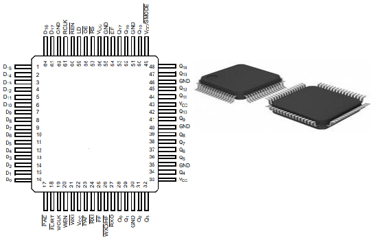
The following figure is the diagram of CY7C4255V Pinout.

Pinout

CY7C4255V CAD Model

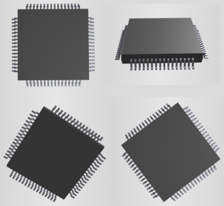
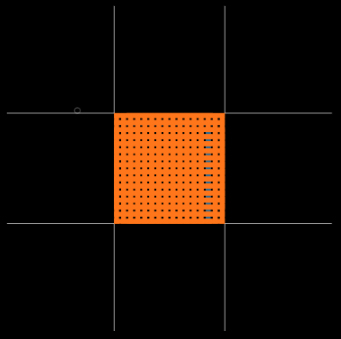
The followings are CY7C4255V Footprint and 3D Model.

Footprint


3D Model

CY7C4255V Description

The CY7C4255V is high speed, low power, first-in first-out (FIFO) memory with clocked read and write interfaces. It is 18 bits wide and is pin and functionally compatible to the CY7C42X5V Synchronous FIFO family. The CY7C4255V can be cascaded to increase FIFO depth. Programmable features include Almost Full/Almost Empty flags. These FIFOs provide solutions for a wide variety of data buffering needs, including high speed data acquisition, multiprocessor interfaces, and communications buffering.

This article provides you with a basic overview of the CY7C4255V Low Voltage Deep Sync FIFOs, including its pin descriptions, features and specifications, etc., to help you quickly understand what CY7C4255V is.

CY7C4255V Features

● 3.3 V operation for low power consumption and easy integration into low voltage systems

● High speed, low power, first-in first-out (FIFO) memories

● 8K × 18

● 0.35 micron CMOS for optimum speed and power

● High speed 100 MHz operation (10 ns read/write cycle times)

● Low power

   ◆ ICC = 30 mA

   ◆ ISB = 4 mA

● Fully asynchronous and simultaneous read and write operation

● Empty, Full, Half Full, and programmable Almost Empty and Almost Full status flags

● Retransmit function

● Output Enable pin

● Independent read and write enable pins

● Supports free running 50% duty cycle clock inputs

● Width Expansion Capability

● Depth Expansion Capability

● 64-pin 10 × 10 STQFP

● Pin compatible density upgrade to CY7C42X5V-ASC families

● Pin compatible 3.3 V solutions for CY7C4255V


Specifications

Cypress Semiconductor Corp CY7C4255V-15ASXC technical specifications, attributes, parameters and parts with similar specifications to Cypress Semiconductor Corp CY7C4255V-15ASXC.

CY7C4255V-15ASXC Tech Specifications

Cypress Semiconductor Corp CY7C4255V-15ASXC technical specifications, attributes, parameters and parts with similar specifications to Cypress Semiconductor Corp CY7C4255V-15ASXC.

Product Attribute Attribute Value
Factory Lead Time13 Weeks
Contact PlatingGold, Tin
MountSurface Mount
Mounting TypeSurface Mount
Package / Case64-LQFP
Number of Pins64Pins
Operating Temperature0°C~70°C
PackagingTray
SeriesCY7C
Published1996
JESD-609 Codee3
Part StatusObsolete
Moisture Sensitivity Level (MSL)3 (168 Hours)
Number of Terminations64Terminations
ECCN CodeEAR99
Terminal FinishMatte Tin (Sn)
Additional FeatureRETRANSMIT
Voltage - Supply3V~3.6V
Terminal PositionQUAD
Product Attribute Attribute Value
Terminal FormGULL WING
Peak Reflow Temperature (Cel)260
Supply Voltage3.3V
Terminal Pitch0.5mm
Frequency66.7MHz
Time@Peak Reflow Temperature-Max (s)20
Base Part Number7C4255
FunctionSynchronous
Operating Supply Voltage3.3V
Supply Voltage-Max (Vsup)3.6V
Supply Voltage-Min (Vsup)3V
Number of Circuits2Circuits
Memory Size144K 8K x 18
Element ConfigurationDual
Nominal Supply Current30mA
Max Supply Current30mA
Access Time10ns
Data Bus Width18b
DirectionUnidirectional
Product Attribute Attribute Value
Organization8KX18
Memory Width18
Density144 kb
Standby Current-Max0.004A
Parallel/SerialPARALLEL
Word Size18b
Memory IC TypeOTHER FIFO
Bus DirectionalUni-Directional
FWFT SupportNo
Programmable Flags SupportYes
Output EnableYES
Expansion TypeDepth, Width
Cycle Time15 ns
Length10mm
Height Seated (Max)1.6mm
RoHS StatusROHS3 Compliant
Lead FreeLead Free
0 Products View Similar

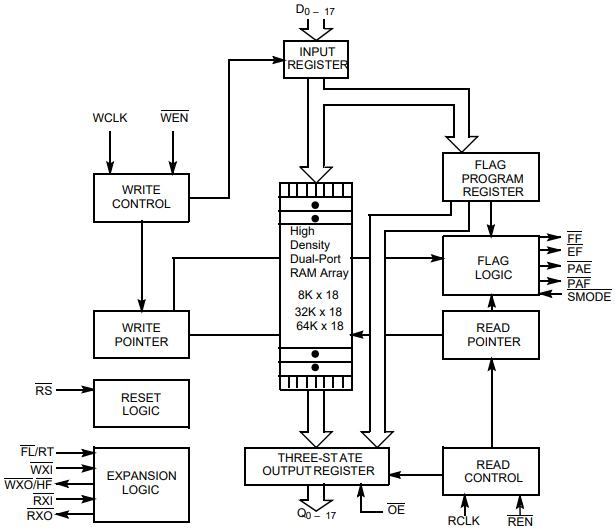
CY7C4255V Functional Block Diagram

The following is the Logic Block Diagram of CY7C4255V.

Logic Block Diagram

CY7C4255V Equivalent

          Model number                     Manufacturer                                           Description
CY7C4255-10AI Cypress Semiconductor FIFO, 8KX18, 8ns, Synchronous, CMOS, PQFP64, 14 X 14 MM, 1.40 MM HEIGHT, PLASTIC, TQFP-64
IDT72255L12TF Integrated Device Technology Inc FIFO, 8KX18, 9ns, Synchronous, CMOS, PQFP64, STQFP-64
CY7C4255-15AXC Cypress Semiconductor FIFO, 8KX18, 10ns, Synchronous, CMOS, PQFP64, 14 X 14 MM, 1.40 MM HEIGHT, LEAD FREE, PLASTIC, TQFP-64
IDT72255L12PF Integrated Device Technology Inc FIFO, 8KX18, 9ns, Synchronous, CMOS, PQFP64, TQFP-64
CY7C4255-35AC Cypress Semiconductor FIFO, 8KX18, 20ns, Synchronous, CMOS, PQFP64, 14 X 14 MM, 1.40 MM HEIGHT, PLASTIC, TQFP-64
CY7C4255V-15ASC Cypress Semiconductor FIFO, 8KX18, 10ns, Synchronous, CMOS, PQFP64, 10 X 10 MM, 1.40 MM HEIGHT, PLASTIC, STQFP-64
CY7C4255V-15ASI Cypress Semiconductor FIFO, 8KX18, 10ns, Synchronous, CMOS, PQFP64, 10 X 10 MM, 1.40 MM HEIGHT, PLASTIC, STQFP-64
CY7C4255V-25ASC Rochester Electronics LLC 8K X 18 OTHER FIFO, 15 ns, PQFP64, 10 X 10 MM, 1.40 MM HEIGHT, PLASTIC, TQFP-64
CY7C4255-10ACT Cypress Semiconductor FIFO, 8KX18, 8ns, Synchronous, CMOS, PQFP64, 14 X 14 MM, 1.40 MM HEIGHT, PLASTIC, TQFP-64

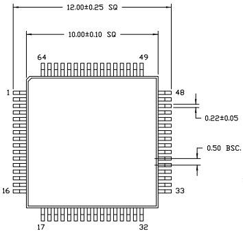
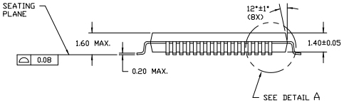
CY7C4255V Package

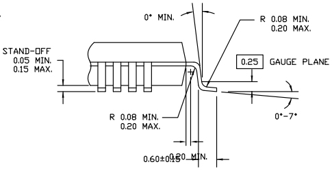
The following diagrams show the CY7C4255V Package.

View A


View B


Detail A

CY7C4255V Manufacturer

Cypress targets innovative markets growing faster than the overall semiconductor industry, including key segments of the automotive, industrial, home automation and appliances, medical products and consumer electronics businesses. With the help of Digi-Key Electronics, we supply customers with market-leading solutions based on our MCUs, wireless SoCs, memories, analog ICs and USB controllers. Our world-class wireless technology gives us an unparalleled position in the fast-growing Internet of Things, a business that cuts across our conventional markets and gives us a stake in exciting, next-generation segments such as connected and autonomous cars.

Datasheet PDF

CY7C4255V-15ASXC Documents

Download datasheets and manufacturer documentation for CY7C4255V-15ASXC

Frequently Asked Questions

How many pins of CY7C4255V-15ASXC?
64 Pins.
What’s the operating temperature of CY7C4255V-15ASXC?
0°C~70°C.
What is the essential property of the CY7C4255V?
The CY7C4255V is high speed, low power, first-in first-out (FIFO) memory with clocked read and write interfaces. It is 18 bits wide and is pin and functionally compatible to the CY7C42X5V Synchronous FIFO family.
How many state pins can the CY7C4255V provide?
The CY7C4255V provides five status pins. These pins are decoded to determine one of five states: Empty, Almost Empty, Half Full, Almost Full, and Full.
How many offset registers does the CY7C4255V device contain?
The CY7C4255V device contains two 16-bit offset registers.
FAQ
How many pins of CY7C4255V-15ASXC?
64 Pins.
What’s the operating temperature of CY7C4255V-15ASXC?
0°C~70°C.
What is the essential property of the CY7C4255V?
The CY7C4255V is high speed, low power, first-in first-out (FIFO) memory with clocked read and write interfaces. It is 18 bits wide and is pin and functionally compatible to the CY7C42X5V Synchronous FIFO family.
How many state pins can the CY7C4255V provide?
The CY7C4255V provides five status pins. These pins are decoded to determine one of five states: Empty, Almost Empty, Half Full, Almost Full, and Full.
How many offset registers does the CY7C4255V device contain?
The CY7C4255V device contains two 16-bit offset registers.

TAGS

Share