ATTENTION: Due to increased demand and order volume, processing time may take an additional 1-3 business days.
HomeCommunitySubjectEP2C35F672I8N FPGA: Features, Specifications and Pins

EP2C35F672I8N FPGA: Features, Specifications and Pins

ALTERA EP2C35F672I8N FPGA, CYCLONE II, 33K ELEMENTS, FBGA672 EP2C35F672I8N is of Cyclone II FPGA Devices.

177

Feb 22, 2021

Rufus

ALTERA EP2C35F672I8N FPGA, CYCLONE II, 33K ELEMENTS, FBGA672

EP2C35F672I8N is of Cyclone II FPGA Devices. To ensure rapid availability and low cost, Cyclone II FPGAs are manufactured on 300-mm wafers using TSMC's 90-nm low-k dielectric process. Cyclone II devices can support complex digital systems on a single chip at a cost comparable to ASICs by minimizing silicon region.

Inquiry
Min.: 1 Mult.: 1
Price not displayed? Not available to buy online? Please send an RFQ, and we will respond immediately.
Quick Links

EP2C35F672I8N Description

EP2C35F672I8N is of Cyclone II FPGA Devices. To ensure rapid availability and low cost, Cyclone II FPGAs are manufactured on 300-mm wafers using TSMC's 90-nm low-k dielectric process. Cyclone II devices can support complex digital systems on a single chip at a cost comparable to ASICs by minimizing silicon region. Unlike other FPGA vendors who compromise power consumption and performance for low-cost, Altera’s latest generation of low-cost FPGAs—Cyclone II FPGAs, offer 60% higher performance and half the power consumption of competing 90-nm FPGAs. The low cost and optimized feature set of Cyclone II FPGAs make them ideal solutions for a wide array of automotive, consumer, communications, video processing, test and measurement, and other end-market solutions. 

EP2C35F672I8N Features

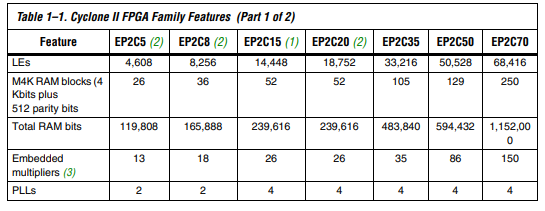
  ■ High-density architecture with 4,608 to 68,416 LEs 

    M4K embedded memory blocks 

    Up to 1.1 Mbits of RAM available without reducing available logic 

    4,096 memory bits per block (4,608 bits per block including 512 parity bits) 

    Variable port configurations of ×1, ×2, ×4, ×8, ×9, ×16, ×18, ×32, and ×36 

    True dual-port (one read and one write, two reads, or two writes) operation for ×1, ×2, ×4, ×8, ×9, ×16, and ×18 modes ● Byte enables for data input masking during writes 

    Up to 260-MHz operation 

  ■ Embedded multipliers 

    Up to 150 18- × 18-bit multipliers are each configurable as two independent 9- × 9-bit multipliers with up to 250-MHz performance 

    Optional input and output registers 

  ■ Advanced I/O support 

    High-speed differential I/O standard support, including LVDS, RSDS, mini-LVDS, LVPECL, differential HSTL, and differential SSTL 

    Single-ended I/O standard support, including 2.5-V and 1.8-V, SSTL class I and II, 1.8-V and 1.5-V HSTL class I and II, 3.3-V PCI and PCI-X 1.0, 3.3-, 2.5-, 1.8-, and 1.5-V LVCMOS, and 3.3-, 2.5-, and 1.8-V LVTTL 

    Peripheral Component Interconnect Special Interest Group (PCI SIG) PCI Local Bus Specification, Revision 3.0 compliance for 3.3-V operation at 33 or 66 MHz for 32- or 64-bit interfaces 

    PCI Express with an external TI PHY and an Altera PCI Express ×1 Megacore® function

    133-MHz PCI-X 1.0 specification compatibility

    High-speed external memory support, including DDR, DDR2, and SDR SDRAM, and QDRII SRAM supported by drop in Altera IP MegaCore functions for ease of use

    Three dedicated registers per I/O element (IOE): one input register, one output register, and one output-enable register

    Programmable bus-hold feature

    Programmable output drive strength feature

    Programmable delays from the pin to the IOE or logic array

    I/O bank grouping for unique VCCIO and/or VREF bank settings

    MultiVolt™ I/O standard support for 1.5-, 1.8-, 2.5-, and 3.3-interfaces

    Hot-socketing operation support

    Tri-state with weak pull-up on I/O pins before and during configuration

    Programmable open-drain outputs

    Series on-chip termination support

  ■ Flexible clock management circuitry 

    Hierarchical clock network for up to 402.5-MHz performance 

    Up to four PLLs per device provide clock multiplication and division, phase shifting, programmable duty cycle, and external clock outputs, allowing system-level clock management and skew control 

    Up to 16 global clock lines in the global clock network that drive throughout the entire device 

  ■ Device configuration 

    Fast serial configuration allows configuration times less than 100 ms 

    Decompression feature allows for smaller programming file storage and faster configuration times 

    Supports multiple configuration modes: active serial, passive serial, and JTAG-based configuration 

    Supports configuration through low-cost serial configuration devices 

    Device configuration supports multiple voltages (either 3.3, 2.5, or 1.8 V) 

  ■ Intellectual property 

    Altera megafunction and Altera MegaCore function support, and Altera Megafunctions Partners Program (AMPPSM) megafunction support, for a wide range of embedded processors, on-chip and off-chip interfaces, peripheral functions, DSP functions, and communications functions and protocols. Visit the Altera IPMegaStore at www.altera.com to download IP MegaCore functions.

    Nios II Embedded Processor support
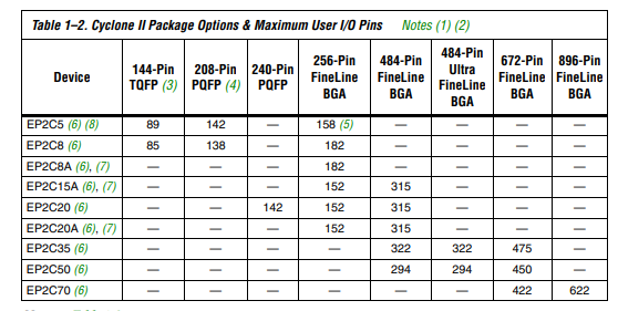
EP2C35F672I8N Pins

Notes: 

(1) Cyclone II devices support vertical migration within the same package (for example, you can migrate between the EP2C20 device in the 484-pin FineLine BGA package and the EP2C35 and EP2C50 devices in the same package). 

(2) The Quartus® II software I/O pin counts include four additional pins, TDI, TDO, TMS, and TCK, which are not available as general purpose I/O pins. 

(3) TQFP: thin quad flat pack. 

(4) PQFP: plastic quad flat pack. 

(5) Vertical migration is supported between the EP2C5F256 and the EP2C8F256 devices. However, not all of the DQ and DQS groups are supported. Vertical migration between the EP2C5 and the EP2C15 in the F256 package is not supported. (6) The I/O pin counts for the EP2C5, EP2C8, and EP2C15A devices include 8 dedicated clock pins that can be used for data inputs. The I/O counts for the EP2C20, EP2C35, EP2C50, and EP2C70 devices include 16 dedicated clock pins that can be used for data inputs. 

(7) EP2C8A, EP2C15A, and EP2C20A have a Fast On feature that has a faster POR time. The EP2C15A is only available with the Fast On option.

Specifications

Altera EP2C35F672I8N technical specifications, attributes, parameters and parts with similar specifications to Altera EP2C35F672I8N.

undefined Tech Specifications

undefined undefined technical specifications, attributes, parameters and parts with similar specifications to undefined undefined.

Product Attribute Attribute Value
0 Products View Similar

Datasheet PDF

Download datasheets and manufacturer documentation for Altera EP2C35F672I8N.

undefined Documents

Download datasheets and manufacturer documentation for

TAGS

Share