ATTENTION: Due to increased demand and order volume, processing time may take an additional 1-3 business days.
HomeCommunitySubjectEPCS16SI8N 3.3V 16 M-bit 8- Pin SOIC Tube, FPGA Configuration Memory

EPCS16SI8N 3.3V 16 M-bit 8- Pin SOIC Tube, FPGA Configuration Memory

ALTERA EPCS16SI8N SERIAL CONFIG MEMORY, 16M, SOIC8, TUBE EPCS16SI8N is an EPCS Flash Serial 3.3V 16M-bit 8-Pin SOIC Tube. This article is going to explain datasheet, replacement, pin configuration about EPCS16SI8N FPGAs.
68

Jan 27, 2022

Vicky Esther

HOW TO CREATE A CPU IN AN FPGA


ALTERA EPCS16SI8N SERIAL CONFIG MEMORY, 16M, SOIC8, TUBE

EPCS16SI8N is an EPCS Flash Serial 3.3V 16M-bit 8-Pin SOIC Tube. This article is going to explain datasheet, replacement, pin configuration about EPCS16SI8N FPGAs.
Inquiry
Min.: 1 Mult.: 1
Price not displayed? Not available to buy online? Please send an RFQ, and we will respond immediately.
Quick Links

What is EPCS16SI8N?

The EPCS16SI8N is an 8-pin SOIC device with a 16-bit serial configuration. After powering up, this EPCS flash memory device can store configuration data for FPGA configuration. It is compatible with any FPGA that supports the ASx1 configuration scheme. Through the Nios processor and SOPC builder, we can access unused memory addresses on the EPCS device to save or retrieve data. Using the JTAG interface, the FPGA may program the EPCS device in-system.

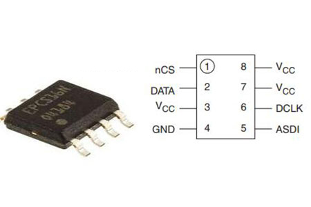
EPCS16SI8N Pinout

EPCS16SI8N Pinout


Pin Name Pin Number in   8-Pin SOIC Package Pin Type Description
DATA 2 Output The DATA output signal transfers data serially out of the EPCS device to the FPGA during the read operation or configuration. During the read operation or configuration,   the EPCS device is enabled by pulling the nCS signal low. The DATA signal transitions on the falling edge of the DCLK signal.
ASDI 5 Input The ASDI signal is used to transfer data serially into the EPCS device. These pins are also receiving data that are programmed into the EPCS device. Data is latched on the rising edge of the DCLK signal.
nCS 1 Input The nCS signal toggles at the beginning and the end of a valid instruction. When this signal goes high, the device is deselected and the DATA pin is tri-stated. When this signal goes low, the device is enabled and in an active mode. After power-up,   the EPCS device requires a falling edge on the nCS signal before the EPCS   device begins any operation.
DCLK 6 Input The FPGA provides the   DCLK signal. This signal provides the timing for the serial interface. The data presented on the ASDI pin is latched to the EPCS device on the rising edge of the DCLK signal. The data on the DATA pin changes after the falling edge of the DCLK signal and is latched into the FPGA on the next falling edge of the DCLK signal.
VCC 3,7,8 Power Connect the power   pins to a 3.3-V power supply
GND 4 GND Ground pin.

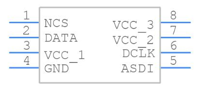
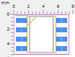
EPCS16SI8N CAD Model

EPCS16SI8N Symbol


EPCS16SI8N  CAD Model


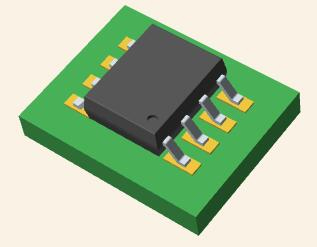
EPCS16SI8N 3D Model

Specifications

Altera EPCS16SI8N technical specifications, attributes, parameters and parts with similar specifications to Altera EPCS16SI8N.

undefined Tech Specifications

undefined undefined technical specifications, attributes, parameters and parts with similar specifications to undefined undefined.

Product Attribute Attribute Value
0 Products View Similar

EPCS16SI8N Features

  • 32 sectors and 512KB per sector

  • ISP support with USB-Blaster, EthernetBlaster or ByteBlaster II download cables

  • Recommended operating voltage of 3.3V

  • Supports active serial (AS) x1 configuration scheme

  • The fast read clock frequency of 40MHz

  • Low cost, low pin count, and non-volatile memory

  • Low current during configuration and near-zero standby mode current

  • Operation voltage range from 2.7V to 3.6V

  • Write protection support for memory sectors using status register bits

  • Operating temperature range from -40°C to 85°C


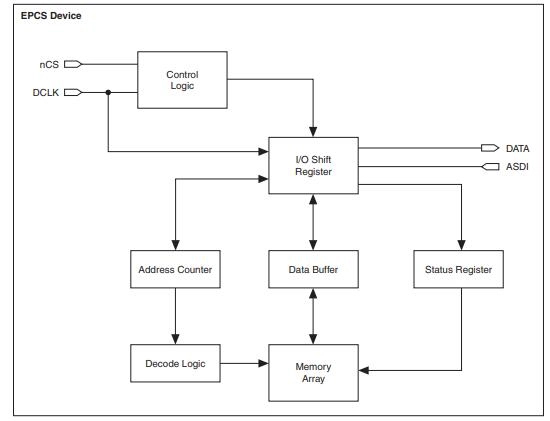
EPCS16SI8N Functional Block Diagram

EPCS16SI8N Functional Block Diagram

EPCS16SI8N Applications

  • Embedded Design & Development

  • Artificial Intelligence

  • 5G Technology

  • Cloud Computing

  • Consumer Electronics

  • Wireless Technology

  • Industrial Control

  • Internet of Things

  • Medical Equipment

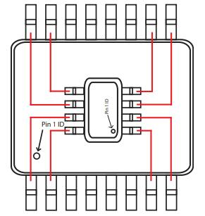
EPCS16SI8N Layout Recommendation

EPCS16SI8N Layout Recommendation

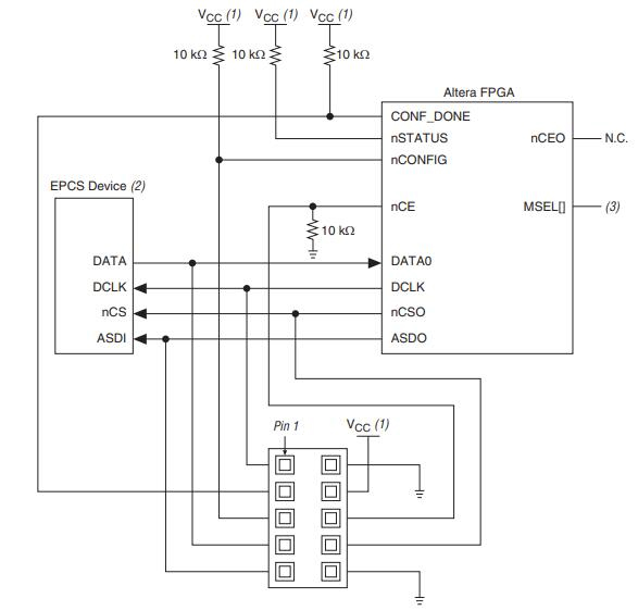
Altera FPGA Configuration in AS Mode Using a Download Cable

Altera FPGA Configuration in AS Mode Using a Download Cable

EPCS16SI8N Manufacturer

Altera Corporation was established in 1983, with the Chinese name: Altera, headquartered in San Jose, California, with more than 2,600 employees in 19 countries, and annual revenue in 2006 reached $ 1.29 billion. Altera is a company specializing in the design, production, and sales of high-performance, high-density programmable logic devices (PLDs) and corresponding development tools.

Datasheet PDF

Download datasheets and manufacturer documentation for Altera EPCS16SI8N.

undefined Documents

Download datasheets and manufacturer documentation for

Frequently Asked Questions

Does the price of EPCS16SI8N devices fluctuate frequently?
The FPGA key search engine tracks the quantity and price of EPCS16SI8N inventory from global electronic component vendors in real-time and saves historical price data regularly. You may look at past price patterns for electronic components to help you make buying decisions.
The FPGA key search engine tracks the quantity and price of EPCS16SI8N inventory from global electronic component vendors in real time, and saves historical price data on a regular basis. You may look at past price patterns for electronic components to help you make buying decisions.
Quartus Prime Modelsim is the corresponding programming software for FPGA produced by Altera/Intel. The specific choice depends on personal habits and functional requirements to specifically select a more suitable match. You can search and download through the FPGA resource channel.
What can be EPCS16SI8N used for?
This EPCS flash memory device can store configuration data for FPGA configuration purposes after power on. It can be used on all FPGA that supports the ASx1 configuration scheme. We can access unused memory locations of EPCS devices to store or retrieve data through the Nios processor and SOPC builder.
What is the voltage of EPCS16SI8N?
3.3V
What is the operating temperature of EPCS16SI8N?
-40°C to 85°C
FAQ
Does the price of EPCS16SI8N devices fluctuate frequently?
The FPGA key search engine tracks the quantity and price of EPCS16SI8N inventory from global electronic component vendors in real-time and saves historical price data regularly. You may look at past price patterns for electronic components to help you make buying decisions.
The FPGA key search engine tracks the quantity and price of EPCS16SI8N inventory from global electronic component vendors in real time, and saves historical price data on a regular basis. You may look at past price patterns for electronic components to help you make buying decisions.
Quartus Prime Modelsim is the corresponding programming software for FPGA produced by Altera/Intel. The specific choice depends on personal habits and functional requirements to specifically select a more suitable match. You can search and download through the FPGA resource channel.
What can be EPCS16SI8N used for?
This EPCS flash memory device can store configuration data for FPGA configuration purposes after power on. It can be used on all FPGA that supports the ASx1 configuration scheme. We can access unused memory locations of EPCS devices to store or retrieve data through the Nios processor and SOPC builder.
What is the voltage of EPCS16SI8N?
3.3V
What is the operating temperature of EPCS16SI8N?
-40°C to 85°C

TAGS

Share