4094 shift register
Logic - Shift Registers 5V SOIC Shift Register 28MHz
The HEF4094BT is an 8-stage serial shift register. This article will unlock its pinout, datasheet, application and functional diagram about HEF4094BT.

Logic - Shift Registers 5V SOIC Shift Register 28MHz The HEF4094BT is an 8-stage serial shift register. This article will unlock its pinout, datasheet, application and functional diagram about HEF4094BT.
273
Dec 17, 2021
Kelly Priestley
4094 shift register
Logic - Shift Registers 5V SOIC Shift Register 28MHz
The HEF4094BT is an 8-stage serial shift register. This article will unlock its pinout, datasheet, application and functional diagram about HEF4094BT.
HEF4094BT
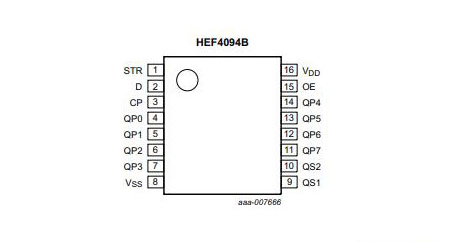
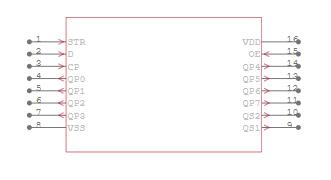
HEF4094BT Symbol
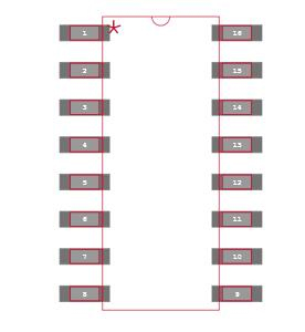
HEF4094BT Footprint
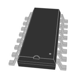
HEF4094BT 3D Model
The HEF4094BT is an 8 -stage serial shift register. It has a storage latch associated with each stage for strobing data from the serial input to parallel buffered 3-state outputs QP0 to QP7. The parallel outputs may be connected directly to common bus lines. Data is shifted on positive-going clock transitions. The data in each shift register stage is transferred to the storage register when the strobe (STR) input is HIGH. Data in the storage register appears at the outputs whenever the output-enable (OE) signal is HIGH.
It operates over a recommended VDD power supply range of 3 V to 15 V referenced to VSS (usually ground). Unused inputs must be connected to VDD, VSS, or another input.
Fully static operation
5 V, 10 V, and 15 V parametric ratings
Standardized symmetrical output characteristics
Specified from -40 ℃ to +85 ℃ and -40 ℃ to +125 ℃
Complies with JEDEC standard JESD 13-B
Some examples of applications for the HEF4094B are:
• Serial-to-parallel data conversion
• Remote control holding register
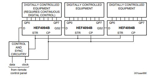
HEF4094BT-Remote control holding register
The following figure shows the functional diagram of HEF4094BT below.
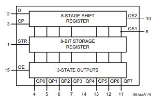
HEF4094BT Functional Diagram
The following figure shows the logic diagram of HEF4094BT below.
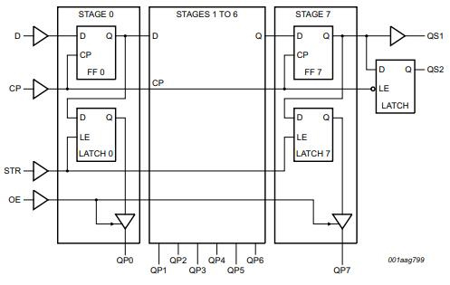
HEF4094BT Logic Diagram
Nexperia HEF4094BT technical specifications, attributes, parameters and parts with similar specifications to Nexperia HEF4094BT.
Nexperia HEF4094BT technical specifications, attributes, parameters and parts with similar specifications to Nexperia HEF4094BT.
| Product Attribute | Attribute Value | |
|---|---|---|
| Package / Case | SOIC | |
| Surface Mount | YES | |
| Number of Pins | 16Pins | |
| Number of Elements | 1 Element | |
| Published | 2013 | |
| JESD-609 Code | e4 | |
| Part Status | Active | |
| Moisture Sensitivity Level (MSL) | 1 (Unlimited) | |
| Number of Terminations | 16Terminations | |
| Terminal Finish | Nickel/Palladium/Gold (Ni/Pd/Au) | |
| Max Operating Temperature | 70°C | |
| Min Operating Temperature | -40°C |
| Product Attribute | Attribute Value | |
|---|---|---|
| Additional Feature | PARALLEL OUTPUT IS LATCHED; UNLATCHED SERIAL SHIFT RIGHT OUTPUT | |
| Terminal Position | DUAL | |
| Terminal Form | GULL WING | |
| Peak Reflow Temperature (Cel) | 260 | |
| Number of Functions | 1Function | |
| Supply Voltage | 5V | |
| Frequency | 28MHz | |
| Time@Peak Reflow Temperature-Max (s) | 30 | |
| Temperature Grade | AUTOMOTIVE | |
| Voltage | 15V | |
| Max Supply Voltage | 15.5V | |
| Min Supply Voltage | 4.5V |
| Product Attribute | Attribute Value | |
|---|---|---|
| Number of Bits | 8Bits | |
| Logic Function | Shift Register | |
| Output Characteristics | 3-STATE | |
| Output Polarity | TRUE | |
| Logic IC Type | SERIAL IN PARALLEL OUT | |
| Trigger Type | POSITIVE EDGE | |
| Propagation Delay (tpd) | 330 ns | |
| Count Direction | RIGHT | |
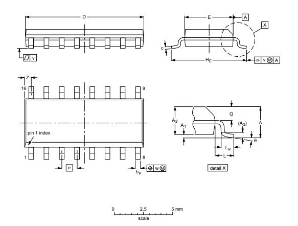
| Length | 9.9mm | |
| Width | 3.9mm | |
| REACH SVHC | No SVHC | |
| RoHS Status | RoHS Compliant |
Nexperia is a dedicated global leader in Discretes, Logic and MOSFETs devices. This new company became independent at the beginning of 2017. Focused on efficiency, Nexperia produces consistently reliable semiconductor components at a high volume: 85 billion annually. The company’s extensive portfolio meets the stringent standards set by the Automotive industry. And industry-leading small packages, produced in their own manufacturing facilities, combine power and thermal efficiency with best-in-class quality levels. Built on over half a century of expertise, Nexperia has 11,000 employees across Asia, Europe and the U.S. supporting customers globally.
The more similar parts come from Nexperia following
HEF4094BT,653
HEF4094B
HEF4094BT,652 and so on
Download datasheets and manufacturer documentation for HEF4094BT
TAGS
Comments