TLP250 Optocoupler Test Circuit, Pinout, How to Test TLP250 Optocoupler
OPTOISO 2.5KV 1CH GATE DRVR 8SMD
TLP250 is an isolated IGBT/Mosfet driver IC. This article mainly covers its pinout, datasheet, how to use TLP250 and more details about TLP250.

OPTOISO 2.5KV 1CH GATE DRVR 8SMD TLP250 is an isolated IGBT/Mosfet driver IC. This article mainly covers its pinout, datasheet, how to use TLP250 and more details about TLP250.
1549
Feb 8, 2022
Daniel Hope
TLP250 Optocoupler Test Circuit, Pinout, How to Test TLP250 Optocoupler
OPTOISO 2.5KV 1CH GATE DRVR 8SMD
TLP250 is an isolated IGBT/Mosfet driver IC. This article mainly covers its pinout, datasheet, how to use TLP250 and more details about TLP250.
TLP250(TP1,F)
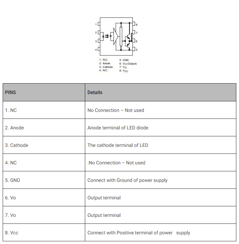
TLP250 is suitable for the gate driving circuit of IGBT or power MOS FET. A GaAlAs light-emitting diode is used on the input side. An integrated photodetector provides a driving signal to the output side. As a result, electrical isolation between low and high power circuits is the most important aspect. It uses light to transmit electrical impulses.
It may be used to drive the gate terminal of high voltage switches in both high and low side drive configurations. It's packaged as an 8-pin DIP chip.
• Input threshold current: 5mA(max)
• Supply current : 11mA(max)
• Supply voltage : 10-35V
• Output current : ±1.5A (max)
• Switching time tpLH/tpHL): 0.5μs(max)
• Isolation voltage: 2500Vrms(min)
• UL -recognized: UL 1577, File No.E67349
• cUL-recognized: CSA Component Acceptance Service No.5A File No.E67349
• VDE-Approved: EN 60747-5- 5 (Note 1)
Induction heating
Solar heating system
Solar inverters/ Power Inverter
Pure sine wave and modified sine wave inverters
There are two stages in the TLP250: an input stage and an output stage. A power supply setup is also included. It is better for MOSFETs and IGBTs. This MOSFET driver is optically isolated, which sets it apart from other MOSFET drivers. Its electrical input and output sides are electrically insulated from one another. However, an optical signal is used to transport electrical signals between the two sides. It functions similarly to an optocoupler. A light-emitting diode is used in the input stage, while a photodiode is used in the output stage, The output gets high whenever the input stage LED light falls on the output stage photodetector diode.
The low-side Mosfet driver circuit employing the TLP250 is illustrated below. The TLP250 is utilized as a non-inverting low-side Mosfet driver in this circuit layout. Between the power source and the electrolytic capacitor, a 0.47 uf electrolytic capacitor should be connected. It protects the TLP250 by giving a constant voltage to the IC.
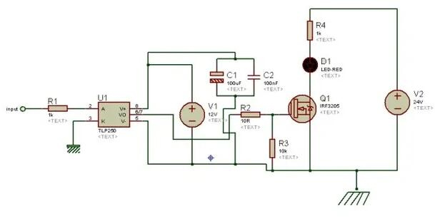
Isolated MOSFET driver TLP250 as a Low Side Driver
Input is a driving signal that drives the output, as indicated in the diagram above. Signal ground is used to calculate Vin. It should be kept away from the supply and output grounds. The load ground is referenced to the power ground and is separated from the input signal reference ground, as indicated in the above figure TLP250. MOSFET Q1 receives a high signal from TLP250 when input is high, and it is powered by a power source, allowing current to flow through the load.
MOSFET Q1 receives a low signal from a TLP250 output pin when input is low, and Mosfet Q1 remains off and no current flows to the load. The supply voltage is typically between 10 -15 volts. Depending on the magnitude of the input signal, the input resistor at the gate of the MOSFET is employed. Typically, the input signal is given by a microcontroller, with a level of 5 volts for the microcontroller input signal. As a decoupling capacitor, capacitor C1 is employed.
The following is a circuit schematic for the TLP250 MOSFET /IGBT driver, which is utilized as a high side driver, It's a high-side gate drive circuit that isn't inverting. Because the input signal ground is linked to the input stage light-emitting diode's cathode. As a result, it's referred to as a non-inverting high-side gate driver.
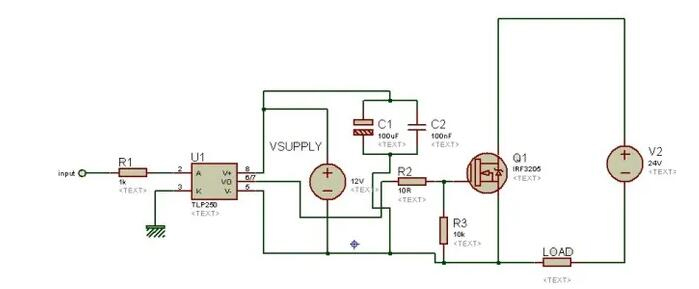
TLP250 as a High Side MOSFET IGBT Driver
As illustrated in the diagram above, there are three grounds in a high side layout. The input signal's ground, the supply voltage's ground, and the power supply voltage's ground. When utilizing the TLP250 as a high-side MOSFET driver. keep in mind that all grounds should be separated from one another.
Toshiba Semiconductor & Storage provides a wide range of supporting technology solutions that enable OEMs, ODMs, CMs, and fabless semiconductor businesses to create innovative integrated products for industries such as computers, networking, communications, digital consumer, automotive, and others.
Toshiba Semiconductor and Storage TLP250(TP1,F) technical specifications, attributes, parameters and parts with similar specifications to Toshiba Semiconductor and Storage TLP250(TP1,F).
Toshiba Semiconductor and Storage TLP250(TP1,F) technical specifications, attributes, parameters and parts with similar specifications to Toshiba Semiconductor and Storage TLP250(TP1,F).
| Product Attribute | Attribute Value | |
|---|---|---|
| Factory Lead Time | 16 Weeks | |
| Mount | Surface Mount | |
| Mounting Type | Surface Mount | |
| Package / Case | 8-SMD, Gull Wing | |
| Number of Pins | 8Pins | |
| Operating Temperature | -20°C~85°C | |
| Packaging | Tape & Reel (TR) | |
| Published | 2009 | |
| Part Status | Last Time Buy |
| Product Attribute | Attribute Value | |
|---|---|---|
| Moisture Sensitivity Level (MSL) | 1 (Unlimited) | |
| Approval Agency | UR | |
| Voltage - Isolation | 2500Vrms | |
| Max Output Current | 1.5A | |
| Number of Channels | 1Channel | |
| Voltage - Forward (Vf) (Typ) | 1.6V | |
| Propagation Delay | 500 ns | |
| Turn On Delay Time | 500 ns | |
| Forward Current | 10mA |
| Product Attribute | Attribute Value | |
|---|---|---|
| Direction | Unidirectional | |
| Output Current per Channel | 1.5A | |
| Current - DC Forward (If) (Max) | 20mA | |
| Propagation Delay tpLH / tpHL (Max) | 500ns, 500ns | |
| Common Mode Transient Immunity (Min) | 5kV/μs | |
| Reverse Voltage (DC) | 5V | |
| Voltage - Output Supply | 15V~30V | |
| RoHS Status | RoHS Compliant | |
| Lead Free | Lead Free |
Download datasheets and manufacturer documentation for Toshiba Semiconductor and Storage TLP250(TP1,F).
Download datasheets and manufacturer documentation for TLP250(TP1,F)
TAGS
Comments