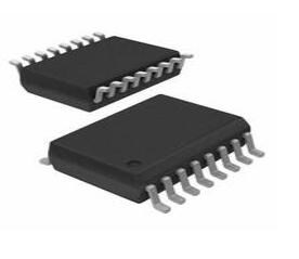
IC INST AMP 1 CIRCUIT 16SOIC
This article will unlock more details about INA115BU, a low cost, general purpose instrumentation amplifier.

IC INST AMP 1 CIRCUIT 16SOIC This article will unlock more details about INA115BU, a low cost, general purpose instrumentation amplifier.
34
Sep 10, 2021
Lee Nahum
IC INST AMP 1 CIRCUIT 16SOIC
This article will unlock more details about INA115BU, a low cost, general purpose instrumentation amplifier.
INA115BUG4
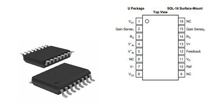
Symbol
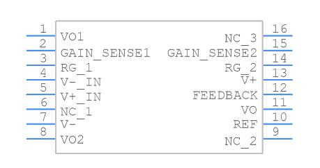
INA115BU Symbol
Footprint
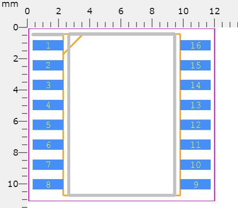
INA115BU Footprint
3D Model
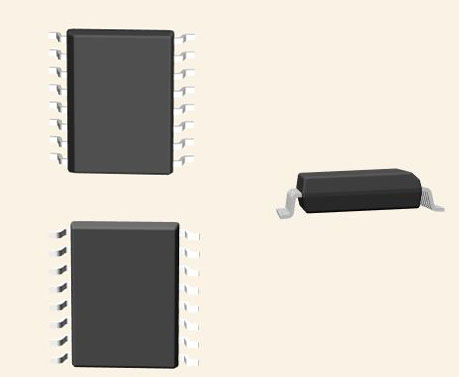
INA115BU 3D Model
The INA115BU is a low cost, general-purpose instrumentation amplifier offering excellent accuracy. Its versatile three-op amp design and small size make it ideal for a wide range of applications. Similar to the model INA114, the INA115BU provides additional connections to the input op-amps, A1 and A2, which improve gain accuracy in high gains and are useful in forming switched-gain amplifiers.
Texas Instruments INA115BUG4 technical specifications, attributes, parameters and parts with similar specifications to Texas Instruments INA115BUG4.
Texas Instruments INA115BUG4 technical specifications, attributes, parameters and parts with similar specifications to Texas Instruments INA115BUG4.
| Product Attribute | Attribute Value | |
|---|---|---|
| Factory Lead Time | 6 Weeks | |
| Mounting Type | Surface Mount | |
| Package / Case | 16-SOIC (0.295, 7.50mm Width) | |
| Surface Mount | YES | |
| Number of Pins | 16Pins | |
| Weight | 420.395078mg | |
| Current - Supply (Nom) | 3mA | |
| Number of Elements | 3 Elements | |
| Operating Temperature | -40°C~85°C | |
| Packaging | Tube | |
| JESD-609 Code | e4 | |
| Part Status | Active | |
| Moisture Sensitivity Level (MSL) | 3 (168 Hours) | |
| Number of Terminations | 16Terminations | |
| ECCN Code | EAR99 | |
| Resistance | 10GOhm | |
| Terminal Finish | Nickel/Palladium/Gold (Ni/Pd/Au) |
| Product Attribute | Attribute Value | |
|---|---|---|
| Voltage - Supply | 15V | |
| Terminal Position | DUAL | |
| Terminal Form | GULL WING | |
| Peak Reflow Temperature (Cel) | 260 | |
| Number of Functions | 1Function | |
| Time@Peak Reflow Temperature-Max (s) | NOT SPECIFIED | |
| Base Part Number | INA115 | |
| Current - Supply (Max) | 3mA | |
| Qualification Status | Not Qualified | |
| Number of Circuits | 1Circuit | |
| Quiescent Current | 2.2mA | |
| Current - Supply | 2.2mA | |
| Slew Rate | 0.6V/μs | |
| Amplifier Type | Instrumentation | |
| Common Mode Rejection Ratio | 110 dB | |
| Current - Input Bias | 500pA | |
| Voltage - Supply, Single/Dual (±) | 4.5V~36V ±2.25V~18V |
| Product Attribute | Attribute Value | |
|---|---|---|
| Output Current per Channel | 20mA | |
| Input Offset Voltage (Vos) | 10μV | |
| Neg Supply Voltage-Nom (Vsup) | -15V | |
| Voltage Gain | 80dB | |
| Average Bias Current-Max (IIB) | 0.002μA | |
| -3db Bandwidth | 1MHz | |
| Dual Supply Voltage | 15V | |
| Input Offset Current-Max (IIO) | 0.002μA | |
| Input Voltage Noise Density | 11nV/sqrt Hz | |
| Voltage Gain-Nom | 10 | |
| Height | 2.35mm | |
| Length | 10.28mm | |
| Width | 7.52mm | |
| RoHS Status | ROHS3 Compliant | |
| Lead Free | Lead Free |
Low offset voltage: 50µV max
Low drift: 0.25µV/°C max
Low input bias current: 2nA max
High common-mode rejection: ±40V
Wide supply range: ±2.25 TO ±18V
Low quiescent current: 3mA max
Sol-16 surface-mount package
Switched-gain amplifier
Bridge amplifier
Thermocouple amplifier
RTD sensor amplifier
Medical instrumentation
Data acquisition
A circuit shows the basic connections required for the operation of the INA115BU. Applications with noisy or high impedance power supplies may require decoupling capacitors close to the device pins as shown.
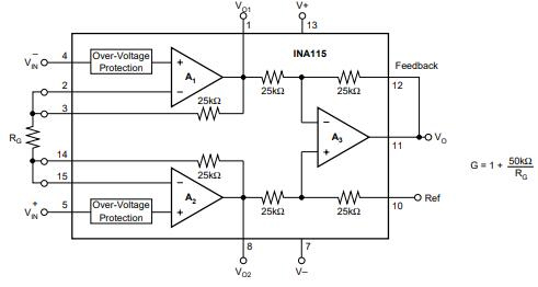
INA115BU Application Circuit
A circuit for the digital selection of four gains is below. Multiplexer “on” resistance does not significantly affect the gain. The resistor values required for some commonly used gain steps are shown. This circuit uses the internal 25kΩ feedback resistors, so the resistor values shown cannot be scaled to a different impedance level.
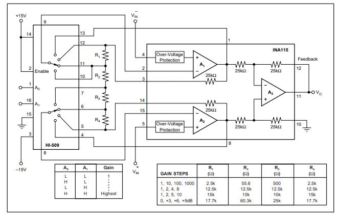
Typical Application Circuit- Switched-Gain Instrumentation Amplifier (minimum components)
A circuit shows an alternative switchable gain configuration. This circuit does not use the internal 25kΩ feedback resistors, so the nominal values shown can be scaled to other impedance levels. This circuit is ideal for use with a precision resistor network to achieve excellent gain accuracy and the lowest gain drift.
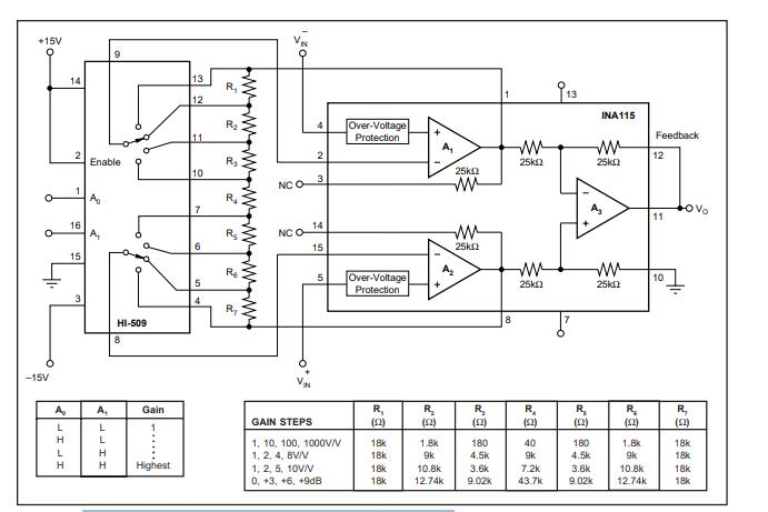
Typical Application Circuit- Switched-Gain Instrumentation Amplifier (improved gain drift)
Texas Instruments (TI) is a global semiconductor firm originating in 1958 and nowadays it has over 30,000 employees who design, conduct and sell analogue and product-differentiating embedded processing components in 35 countries. Aimed at changing the world of tech, TI has put great effort into becoming the solution provider coupled with a vision.
Download datasheets and manufacturer documentation for INA115BUG4
TAGS
Comments