Using IRF520 MOSFET Switch Button to Turn ON or OFF DC load
MOSFET N-CH 100V 10A TO-220
The IRF520 is an N-Channel Power Mosfet that's been designed to minimize input capacitance and gate charge.

MOSFET N-CH 100V 10A TO-220 The IRF520 is an N-Channel Power Mosfet that's been designed to minimize input capacitance and gate charge.
290
Jul 29, 2021
Jonas Kathleen
Using IRF520 MOSFET Switch Button to Turn ON or OFF DC load
MOSFET N-CH 100V 10A TO-220
The IRF520 is an N-Channel Power Mosfet that's been designed to minimize input capacitance and gate charge.
IRF520
The IRF520 is an N-Channel Power Mosfet that's been designed to minimize input capacitance and gate charge. It is therefore suitable as primary switch in advanced high-efficiency, high-frequency isolated DC-DC converters for Telecom and Computer applications. The IRF520 is also intended for any applications with low gate drive requirements.
The IRF520 is a right MOSFET if you are looking to drive the output of an IC or from a platform like Arduino or Raspberry Pi. The maximum load this transistor can drive is 9.2A with the maximum load voltage of upto 100V. The transistor is also a high speed switching device due to which it can be used in any application where the switching speed is very important for example in UPS circuits. Moreover it can also drive a load of upto 37A in pulse mode.
On the other hand the max power dissipation of 60 watts also makes it ideal to use in audio amplifier circuit and in audio amplifier circuit stages.

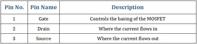
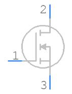
Symbol
Footprint

3D Model
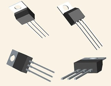
Package Type: TO-220
Transistor Type: N Channel
Drain to Source Breakdown Voltage: 100 V
Gate to Source Voltage: ±20 V
Continuous Drain Current (ID): 9.2 A
Max Power Dissipation: 60 W
Drain Source Resistance (RDS): 0.27 Ohms
Gate threshold voltage (VGS-th): 4 V (max)
Rise time and fall time: 30 nS and 20 nS
Storage & Operating temperature: -55 to +175 Celsius
Typical RDS(on) = 0.115Ω
Avalanche rugged technology
100% avalanche tested
Low gate charge
High current capability
175 oC operating temperature
STMicroelectronics IRF520 technical specifications, attributes, parameters and parts with similar specifications to STMicroelectronics IRF520.
STMicroelectronics IRF520 technical specifications, attributes, parameters and parts with similar specifications to STMicroelectronics IRF520.
| Product Attribute | Attribute Value | |
|---|---|---|
| Mounting Type | Through Hole | |
| Package / Case | TO-220-3 | |
| Surface Mount | NO | |
| Number of Pins | 3Pins | |
| Transistor Element Material | SILICON | |
| Current - Continuous Drain (Id) @ 25℃ | 10A Tc | |
| Drive Voltage (Max Rds On, Min Rds On) | 10V | |
| Number of Elements | 1 Element | |
| Power Dissipation (Max) | 60W Tc | |
| Voltage - Gate Threshold (Vgs(th)) (Max) @ Id | 4V @ 250μA | |
| Operating Temperature | -55°C~175°C TJ | |
| Packaging | Tube | |
| Series | STripFET™ II | |
| JESD-609 Code | e3 | |
| Part Status | Obsolete | |
| Moisture Sensitivity Level (MSL) | 1 (Unlimited) |
| Product Attribute | Attribute Value | |
|---|---|---|
| Number of Terminations | 3Terminations | |
| ECCN Code | EAR99 | |
| Terminal Finish | Matte Tin (Sn) | |
| Additional Feature | FAST SWITCHING | |
| Terminal Position | SINGLE | |
| Peak Reflow Temperature (Cel) | NOT SPECIFIED | |
| Time@Peak Reflow Temperature-Max (s) | NOT SPECIFIED | |
| Base Part Number | IRF5 | |
| JESD-30 Code | R-PSFM-T3 | |
| Qualification Status | Not Qualified | |
| Configuration | SINGLE WITH BUILT-IN DIODE | |
| Operating Mode | ENHANCEMENT MODE | |
| FET Type | N-Channel | |
| Transistor Application | SWITCHING | |
| Rds On (Max) @ Id, Vgs | 270m Ω @ 7A, 10V | |
| Input Capacitance (Ciss) (Max) @ Vds | 460pF @ 25V |
| Product Attribute | Attribute Value | |
|---|---|---|
| Gate Charge (Qg) (Max) @ Vgs | 22nC @ 10V | |
| Drain to Source Voltage (Vdss) | 100V | |
| Vgs (Max) | ±20V | |
| JEDEC-95 Code | TO-220AB | |
| Drain Current-Max (Abs) (ID) | 10A | |
| Drain-source On Resistance-Max | 0.27Ohm | |
| Pulsed Drain Current-Max (IDM) | 40A | |
| DS Breakdown Voltage-Min | 100V | |
| Avalanche Energy Rating (Eas) | 100 mJ | |
| Feedback Cap-Max (Crss) | 100 pF | |
| Turn Off Time-Max (toff) | 50ns | |
| Turn On Time-Max (ton) | 115ns | |
| REACH SVHC | not_compliant | |
| RoHS Status | Non-RoHS Compliant |

IRF520 Unclamped Inductive Load Test Circuit
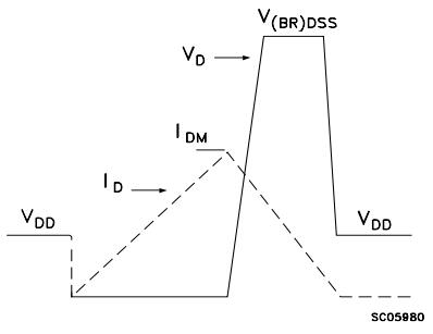
IRF520 Unclamped Inductive Waveform

IRF520 Switching Times Test Circuits For Resistive Load
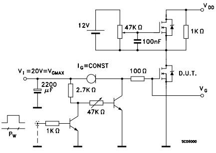
IRF520 Gate Charge Test Circuit

IRF520 Test Circuit For Inductive Load Switching And Diode Recovery Times
The IRF520 can be used in wide variety of circuits such as motor controller circuits, audio amplifier circuits, low current UPS, and power supplies. Besides that it can also be used to drive other high power components such as relays and transistors etc. Due to low gate power requirements it can easily be used at the output of arduino, raspberry pi and a variety of ICs and microcontrollers to drive high current loads.
DC to DC & DC to AC converters
High Speed switching applications
Uninterruptible power supplies
Battery chargers
Battery management systems
Solar Applications
Motor Driver Circuits
Computer & telecommunication applications
LED dimmers or flashers
Audio Amplifiers
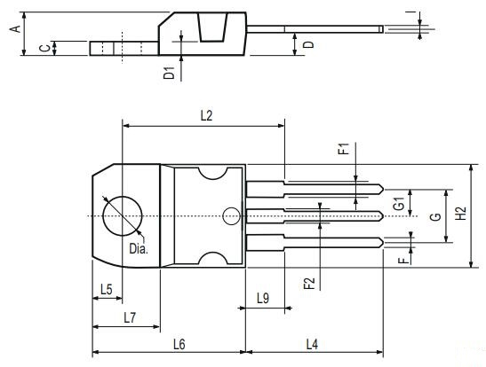
IRF520 Package Outline
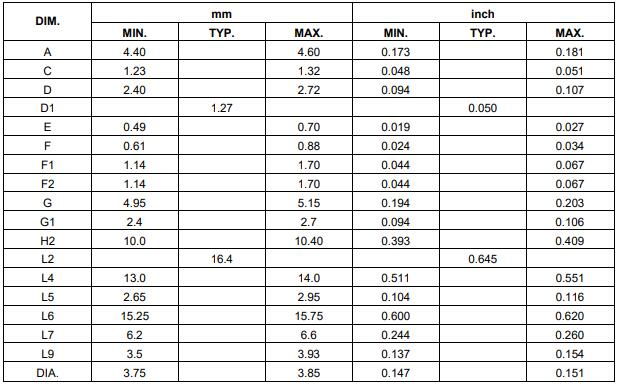
IRF520 Mechanical Data
STMicroelectronics is a global independent semiconductor company and is a leader in developing and delivering semiconductor solutions across the spectrum of microelectronics applications. An unrivaled combination of silicon and system expertise, manufacturing strength, Intellectual Property (IP) portfolio and strategic partners positions the Company at the forefront of System-on-Chip (SoC) technology and its products play a key role in enabling today's convergence trends.
Download datasheets and manufacturer documentation for STMicroelectronics IRF520.
Download datasheets and manufacturer documentation for IRF520
TAGS
Comments