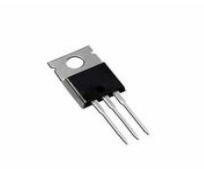
IRF5210 is a 40A 100V P-Channel Power MOSFET. This article mainly covers its pinout, datasheet, application and more information about IRF5210.

IRF5210 is a 40A 100V P-Channel Power MOSFET. This article mainly covers its pinout, datasheet, application and more information about IRF5210.
3950
Feb 24, 2022
Vera Becky
IRF5210 is a 40A 100V P-Channel Power MOSFET. This article mainly covers its pinout, datasheet, application and more information about IRF5210.
IRF5210PBF
| Quantity | Unit Price | Ext. Price |
|---|---|---|
| 1+ | $3.03542 | $3.04 |
| 10+ | $2.8636 | $28.64 |
| 100+ | $2.70151 | $270.15 |
| 500+ | $2.5486 | $1274.3 |
| 1000+ | $2.40433 | $2404.33 |

IRF5210 Pinout
Symbol

irf5210 Symbol
Footprint

IRF5210 Footprint
3D Model

IRF5210 3D Model
Advanced processing techniques were used to create extraordinarily low on-resistance per silicon area in the IRF5210 40 A 100 V P-Channel Power MOSFET. This feature, when paired with the quick switching speed and ruggedized device architecture that HEXFET Power MOSFET s are known for, gives the designer an exceptionally efficient and dependable device that can be used in a broad range of applications. At power dissipation values of around 50 watts, the TO-220 package is widely recommended for all commercial-industrial applications.
Advanced Process Technology
Ultra-Low On-Resistance
Dynamic DV/DT Rating
175°C Operating Temperature
Fast Switching
P-Channel
Fully Avalanche Rated
Switching applications
The equivalent for IRF5210:
IRF034, IRF044, IRF044SMD, IRF054, IRF054SMD, IRF100B201
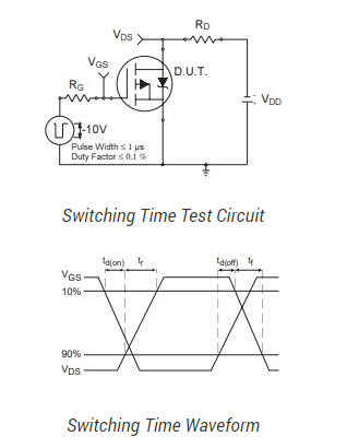
IRF5210 Test Circuit is shown below

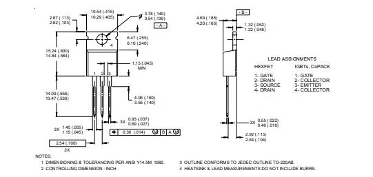
IRF5210 Package
On April 1st, 1999, Siemens Semiconductors became Infineon Technologies. A dynamic more flexible company geared towards success in the competitive, ever-changing world of microelectronics. Infineon is a leading global designer, manufacturer and supplier of a broad range of semiconductors used in various microelectronic applications. Infineon's product portfolio consists of logic products, including digital, mixed-signal, and analogue integrated circuits, as well as discrete semiconductor products.
Infineon Technologies IRF5210PBF technical specifications, attributes, parameters and parts with similar specifications to Infineon Technologies IRF5210PBF.
| Product Attribute | Attribute Value | |
|---|---|---|
| Factory Lead Time | 12 Weeks | |
| Contact Plating | Tin | |
| Mount | Through Hole | |
| Mounting Type | Through Hole | |
| Package / Case | TO-220-3 | |
| Number of Pins | 3Pins | |
| Transistor Element Material | SILICON | |
| Current - Continuous Drain (Id) @ 25℃ | 40A Tc | |
| Drive Voltage (Max Rds On, Min Rds On) | 10V | |
| Number of Elements | 1 Element | |
| Power Dissipation (Max) | 200W Tc | |
| Turn Off Delay Time | 79 ns | |
| Voltage - Gate Threshold (Vgs(th)) (Max) @ Id | 4V @ 250μA | |
| Operating Temperature | -55°C~175°C TJ | |
| Packaging | Tube | |
| Series | HEXFET® | |
| Published | 1998 | |
| JESD-609 Code | e3 | |
| Part Status | Active | |
| Moisture Sensitivity Level (MSL) | 1 (Unlimited) | |
| Number of Terminations | 3Terminations |
| Product Attribute | Attribute Value | |
|---|---|---|
| Termination | Through Hole | |
| ECCN Code | EAR99 | |
| Resistance | 60mOhm | |
| Additional Feature | AVALANCHE RATED, HIGH RELIABILITY, ULTRA LOW RESISTANCE | |
| Voltage - Rated DC | -100V | |
| Peak Reflow Temperature (Cel) | 250 | |
| Current Rating | -40A | |
| Time@Peak Reflow Temperature-Max (s) | 30 | |
| Lead Pitch | 2.54mm | |
| Number of Channels | 1Channel | |
| Element Configuration | Single | |
| Operating Mode | ENHANCEMENT MODE | |
| Power Dissipation | 200W | |
| Case Connection | DRAIN | |
| Turn On Delay Time | 17 ns | |
| FET Type | P-Channel | |
| Transistor Application | SWITCHING | |
| Rds On (Max) @ Id, Vgs | 60m Ω @ 24A, 10V | |
| Input Capacitance (Ciss) (Max) @ Vds | 2700pF @ 25V | |
| Gate Charge (Qg) (Max) @ Vgs | 180nC @ 10V | |
| Rise Time | 86ns |
| Product Attribute | Attribute Value | |
|---|---|---|
| Drain to Source Voltage (Vdss) | 100V | |
| Vgs (Max) | ±20V | |
| Fall Time (Typ) | 81 ns | |
| Continuous Drain Current (ID) | -40A | |
| Threshold Voltage | -4V | |
| JEDEC-95 Code | TO-220AB | |
| Gate to Source Voltage (Vgs) | 20V | |
| Drain to Source Breakdown Voltage | -100V | |
| Dual Supply Voltage | -100V | |
| Avalanche Energy Rating (Eas) | 780 mJ | |
| Recovery Time | 260 ns | |
| Max Junction Temperature (Tj) | 175°C | |
| Nominal Vgs | -4 V | |
| Height | 19.8mm | |
| Length | 10.5156mm | |
| Width | 4.69mm | |
| REACH SVHC | No SVHC | |
| Radiation Hardening | No | |
| RoHS Status | ROHS3 Compliant | |
| Lead Free | Lead Free |
Download datasheets and manufacturer documentation for IRF5210PBF
TAGS
Comments