Top 5 Electronics Projects using IRF540 | irf540 top circuits
MOSFET N-CH 100V 22A TO-220
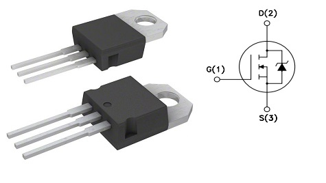
The IRF540 is a common N-channel enhancement MOSFET that's popular among hobbyists and electronic designers.

MOSFET N-CH 100V 22A TO-220 The IRF540 is a common N-channel enhancement MOSFET that's popular among hobbyists and electronic designers.
396
Aug 4, 2021
Fritz
Top 5 Electronics Projects using IRF540 | irf540 top circuits
MOSFET N-CH 100V 22A TO-220
The IRF540 is a common N-channel enhancement MOSFET that's popular among hobbyists and electronic designers.
IRF540
The IRF540 is a common N-channel enhancement MOSFET that's popular among hobbyists and electronic designers. The low thermal resistance and low package cost of the TO-220AB make it a favorite in the industry. The IRF540 is designed to drive high current loads. It can handle a maximum load of upto 23A and the maximum load voltage is upto 100V DC. Its trench technology makes it capable of reaching high-level driving capability. It can be used for both switching and amplification purposes. It is capable of performing high-speed switching. Therefore, it can be used in a wide variety of applications where you want to switch the load with high speed such as UPS.
The IRF540 can also be used as an amplifier, the maximum power dissipation of 100W makes it ideal to build a high power audio amplifier, and it can also be used in high power audio amplifier stages.
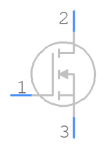
Symbol
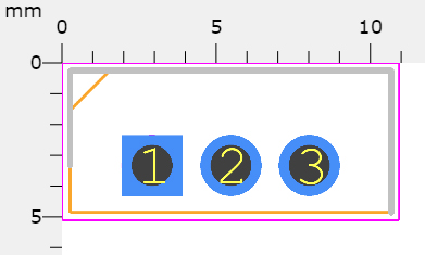
Footprint
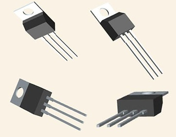
3D Model
Package Type: TO-220
Transistor Type: N Channel
Max Drain to Source Voltage: 100 V
Max Gate to Source Voltage: ±20 V
Max Continues Drain Current: 23 A (Different manufacturers have slightly different ratings of continuous drain current)
Max Pulsed Drain Current: 92 A (Different manufacturers have slightly different ratings of continuous drain current)
Max Power Dissipation: 100 W
Minimum Voltage Required to Conduct: 2 V to 4 V
Storage & Operating temperature: -55 to +150 Celsius
Typical RDS(on) = 0.055Ω
Exceptional dv/dt capability
100% avalanche tested
Low gate charge
Application-oriented characterization
Simple drive requirements
Ease of paralleling
Fast switching
STMicroelectronics IRF540 technical specifications, attributes, parameters and parts with similar specifications to STMicroelectronics IRF540.
STMicroelectronics IRF540 technical specifications, attributes, parameters and parts with similar specifications to STMicroelectronics IRF540.
| Product Attribute | Attribute Value | |
|---|---|---|
| Mount | Through Hole | |
| Mounting Type | Through Hole | |
| Package / Case | TO-220-3 | |
| Number of Pins | 3Pins | |
| Transistor Element Material | SILICON | |
| Current - Continuous Drain (Id) @ 25℃ | 22A Tc | |
| Drive Voltage (Max Rds On, Min Rds On) | 10V | |
| Number of Elements | 1 Element | |
| Power Dissipation (Max) | 85W Tc | |
| Turn Off Delay Time | 50 ns | |
| Voltage - Gate Threshold (Vgs(th)) (Max) @ Id | 4V @ 250μA | |
| Operating Temperature | -55°C~175°C TJ | |
| Packaging | Tube | |
| Series | STripFET™ II | |
| JESD-609 Code | e3 | |
| Part Status | Obsolete | |
| Moisture Sensitivity Level (MSL) | 1 (Unlimited) |
| Product Attribute | Attribute Value | |
|---|---|---|
| Number of Terminations | 3Terminations | |
| ECCN Code | EAR99 | |
| Terminal Finish | Matte Tin (Sn) | |
| Voltage - Rated DC | 100V | |
| Peak Reflow Temperature (Cel) | NOT SPECIFIED | |
| Current Rating | 22A | |
| Time@Peak Reflow Temperature-Max (s) | NOT SPECIFIED | |
| Base Part Number | IRF5 | |
| JESD-30 Code | R-PSFM-T3 | |
| Qualification Status | Not Qualified | |
| Voltage | 100V | |
| Element Configuration | Single | |
| Current | 33A | |
| Operating Mode | ENHANCEMENT MODE | |
| Power Dissipation | 85W | |
| FET Type | N-Channel | |
| Transistor Application | SWITCHING |
| Product Attribute | Attribute Value | |
|---|---|---|
| Rds On (Max) @ Id, Vgs | 77m Ω @ 11A, 10V | |
| Input Capacitance (Ciss) (Max) @ Vds | 870pF @ 25V | |
| Gate Charge (Qg) (Max) @ Vgs | 41nC @ 10V | |
| Rise Time | 45ns | |
| Vgs (Max) | ±20V | |
| Fall Time (Typ) | 20 ns | |
| Continuous Drain Current (ID) | 22A | |
| JEDEC-95 Code | TO-220AB | |
| Gate to Source Voltage (Vgs) | 20V | |
| Drain-source On Resistance-Max | 0.077Ohm | |
| Drain to Source Breakdown Voltage | 100V | |
| Avalanche Energy Rating (Eas) | 220 mJ | |
| Turn Off Time-Max (toff) | 230ns | |
| REACH SVHC | not_compliant | |
| RoHS Status | Non-RoHS Compliant | |
| Lead Free | Contains Lead |
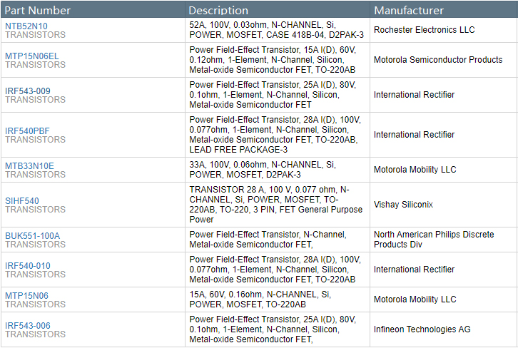
The IRF540 is an N-channel MOSFET that can be widely used in switching and amplification applications. As a switch, it can be used as power supplies, battery management applications, DC to DC converters, etc. It can also be used at the output of microcontrollers and electronic platforms like Arduino and raspberry pi to drive high ampere loads. Other than that, it can also be used to build high-power audio amplifiers.
The way to use MOSFET and BJT is almost the same, the only difference is that MOSFET is the voltage-controlled device, and BJT is a current-controlled device. So MOSFET doesn't require current at its Gate. You can control them by voltage. The minimum voltage IRF540 required for saturation is 2V to 4V.
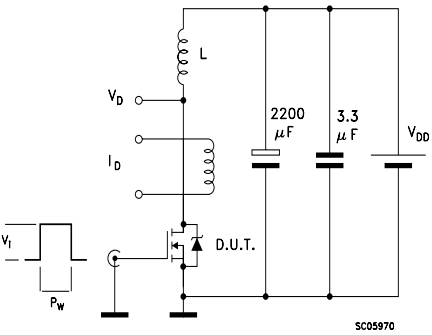
IRF540 Unclamped Inductive Load Test Circuit
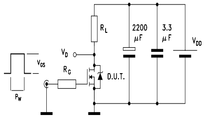
IRF540 Switching Times Test Circuits For Resistive Load

IRF540 Test Circuit For Inductive Load Switching And Diode Recovery Times
Fast Switching Applications
Uninterruptible Power Supplies
Battery Chargers
Battery Management Systems
Solar Battery Chargers
Solar Uninterruptible Power Supplies
Motor Driver Applications
Telecommunication Applications
Computer Related Applications
High-efficiency DC-DC converters

IRF540 Package Outline
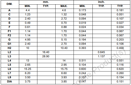
IRF540 Mechanical Data
STMicroelectronics is a global independent semiconductor company and is a leader in developing and delivering semiconductor solutions across the spectrum of microelectronics applications. An unrivaled combination of silicon and system expertise, manufacturing strength, Intellectual Property (IP) portfolio and strategic partners positions the Company at the forefront of System-on-Chip (SoC) technology and its products play a key role in enabling today's convergence trends.
Download datasheets and manufacturer documentation for STMicroelectronics IRF540.
Download datasheets and manufacturer documentation for IRF540
TAGS
Comments