ATTENTION: Due to increased demand and order volume, processing time may take an additional 1-3 business days.
HomeCommunitySubjectIRF830 Power MOSFET: Pinout, Datasheet, and Test Circuit

IRF830 Power MOSFET: Pinout, Datasheet, and Test Circuit

MOSFET N-CH 500V 4.5A TO-220 The IRF830 is a fast switching high voltage N-Channel Power MOSFET with a low on-state resistance.

153

Jul 9, 2021

Elliot Pitman

100V IRF530 Mosfet compared to 500V IRF830 Mosfet


MOSFET N-CH 500V 4.5A TO-220

The IRF830 is a fast switching high voltage N-Channel Power MOSFET with a low on-state resistance.

IRF830

25000In Stock
Min.: 1 Mult.: 1
Price not displayed? Not available to buy online? Please send an RFQ, and we will respond immediately.
Quick Links

IRF830 Description

The IRF830 is a fast switching high voltage N-Channel Power MOSFET with a low on-state resistance. The MOSFET has a maximum drain to source voltage of 500V. The MOSFET will have a drain to source internal resistance of 1.5Ω when triggered with 10V gate voltage. It can withstand a specified level of energy in the breakdown avalanche mode of operation and is designed for applications such as switching regulators, switching converters, motor drivers, relay drivers, and drivers for high power bipolar switching transistors requiring high speed and low gate drive power. The IRF830 can be operated directly from integrated circuits.
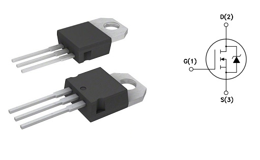
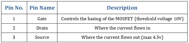
 

IRF830 Pinout

IRF830 Features

  • Package: TO-220

  • Type of Transistor: MOSFET

  • Type of Control Channel: N-Channel

  • Max Power Dissipation (Pd): 75 W

  • Max Drain-Source Voltage |Vds|: 500 V

  • Max Gate-Source Voltage |Vgs|: ±20 V

  • Max Gate-Threshold Voltage |Vgs(th)|: 4 V

  • Max Drain Current |Id|: 4.5A

  • Max Junction Temperature (Tj): 150 °C

  • Total Gate Charge (Qg): 22 nC

  • Drain-Source Capacitance (Cd): 800 pF

  • Max Drain-Source On-State Resistance (Rds): 1.5 Ohm

  • Max Storage & Operating temperature: -55 to +150 °C


IRF830 Advantages

  • Dynamic dV/dt rating

  • Repetitive avalanche rated

  • Fast switching

  • Ease of paralleling

  • Simple drive requirements

Specifications

STMicroelectronics IRF830 technical specifications, attributes, parameters and parts with similar specifications to STMicroelectronics IRF830.

IRF830 Tech Specifications

STMicroelectronics IRF830 technical specifications, attributes, parameters and parts with similar specifications to STMicroelectronics IRF830.

Product Attribute Attribute Value
MountThrough Hole
Mounting TypeThrough Hole
Package / CaseTO-220-3
Transistor Element MaterialSILICON
Current - Continuous Drain (Id) @ 25℃4.5A Tc
Drive Voltage (Max Rds On, Min Rds On)10V
Number of Elements1 Element
Power Dissipation (Max)100W Tc
Operating Temperature150°C TJ
PackagingTube
SeriesPowerMESH™
JESD-609 Codee3
Part StatusObsolete
Moisture Sensitivity Level (MSL)1 (Unlimited)
Number of Terminations3Terminations
Terminal FinishMatte Tin (Sn)
Product Attribute Attribute Value
Additional FeatureHIGH VOLTAGE, FAST SWITCHING
Voltage - Rated DC500V
Current Rating4.5A
Base Part NumberIRF8
Pin Count3
JESD-30 CodeR-PSFM-T3
Element ConfigurationSingle
Operating ModeENHANCEMENT MODE
Power Dissipation100W
Turn On Delay Time11.5 ns
FET TypeN-Channel
Transistor ApplicationSWITCHING
Rds On (Max) @ Id, Vgs1.5 Ω @ 2.7A, 10V
Vgs(th) (Max) @ Id4V @ 250μA
Input Capacitance (Ciss) (Max) @ Vds610pF @ 25V
Gate Charge (Qg) (Max) @ Vgs30nC @ 10V
Product Attribute Attribute Value
Rise Time8ns
Vgs (Max)±20V
Fall Time (Typ)5 ns
Continuous Drain Current (ID)4.5A
JEDEC-95 CodeTO-220AB
Gate to Source Voltage (Vgs)20V
Drain to Source Breakdown Voltage500V
Pulsed Drain Current-Max (IDM)18A
Avalanche Energy Rating (Eas)290 mJ
Feedback Cap-Max (Crss)55 pF
Turn On Time-Max (ton)102ns
Radiation HardeningNo
RoHS StatusNon-RoHS Compliant
Lead FreeContains Lead
0 Products View Similar

IRF830 Test Circuits

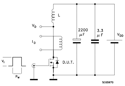
Figure 1: Unclamped Inductive Load Test Circuit
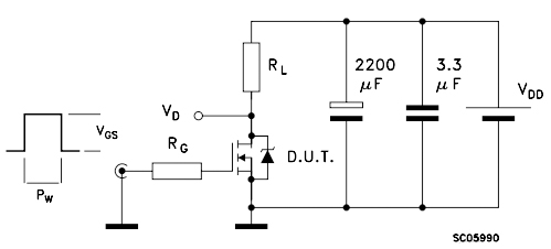
 

Figure 2: Switching Times Test Circuits For Resistive Load
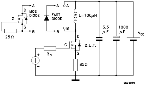
 

Figure 3: Test Circuit For Inductive Load Switching And Diode Recovery Times

Where to use IRF830

IRF830 can be used in many settings. For example, it can be used in high voltage circuits, high speed applications, motor drivers and in any general purpose applications which fall under its ratings. It can also be used at the output of ICs, Microcontroller and electronic platforms as described above. Also, it can be used to build high power audio amplifiers.

IRF830 Applications

  • High current, high speed switching

  • Swith mode power supplies (smps)

  • DC-AC converters for welding equipment and uninterruptible power supplies and motor driver

  • Switching high power devices

  • Inverter Circuits

  • DC-DC Converters

  • Control speed of motors

  • LED dimmers or flashers

IRF830 Package

IRF830 Package Outline


IRF830 Mechanical Data

IRF830 Manufacturer

STMicroelectronics is a global independent semiconductor company and is a leader in developing and delivering semiconductor solutions across the spectrum of microelectronics applications. An unrivaled combination of silicon and system expertise, manufacturing strength, Intellectual Property (IP) portfolio and strategic partners positions the Company at the forefront of System-on-Chip (SoC) technology and its products play a key role in enabling today's convergence trends.


Datasheet PDF

Download datasheets and manufacturer documentation for STMicroelectronics IRF830.

IRF830 Documents

Download datasheets and manufacturer documentation for IRF830

Frequently Asked Questions

1.What is IRF830?
The IRF830 is a fast switching high voltage N-Channel MOSFET with a low on-state resistance. The MOSFET has a maximum drain to source voltage of 500V. The MOSFET will have a drain to source internal resistance of 1.5Ω when triggered with 10V gate voltage.
2.What is IRF in Mosfet?
It is basically an N-Channel power Metal Oxide Silicon Field Effect Transistor (MOSFET) and operates in enhancement mode.
3.What is an N-channel Mosfet?
An N-Channel MOSFET is a type of MOSFET in which the channel of the MOSFET is composed of a majority of electrons as current carriers. When the MOSFET is activated and is on, the majority of the current flowing are electrons moving through the channel.
4.I'm working on a project and I need to switch IRF830 N-Channel MOSFET at roughly 100KHz as low-side. So, how much output current I need to drive this MOSFET 4 in parallel?
First, gate drive current is not typically chosen to just meet the capacitance of the MOSFET. Instead the drive is selected to move the gate voltage as quickly as necessary to maximize the switching efficiency of the circuit. This is why even small gate drivers are specified to deliver a few Amps (in a brief pulse). Now let me answer your question. The datasheet shows Qg = 38 nC with Vgs ending at 10 V and Vds starting at 400 V. Of this 5 nC is Qgs and 22 nC is Qgd. Roughly speaking the gate driver has to drive 2 capacitors. One between Gate and Drain and one between Gate and Source. I tried a simple diagram below. Vdrive --| Cgd |-- Drain Vdrive --| Cgs |-- Source The capacitance is junction and oxide capacitance so it is not constant but changes significantly -- Cgd especially -- with voltage. This is why both gate charge and gate capacitance are given. Assume the drive is 10 V then 5 nC is put onto the gate 100 k times a second = 5 uA. For the gate charge only. The gate to drain capacitance dominates but the drain is probably not a fixed voltage so this an calculation is an estimate. With the scant information provided it's a wild guess. But 38 nC * 100 kHz = 3.8 mA. Of course scale all this up by 4 when you put 4 FETs in parallel.
5.How to safely long run IRF830 in a Circuit?
For long life performance it is suggested to not use this transistor on its max limits. Using a component on its max limits can provide stress on a component and may result internal and outer damage of the component. Therefore we suggest using a component at least 20% below from its maximum ratings. The max drains to source current is 4.5A, therefore do not drive load more than 3.6A. The max drain to source voltage is 500V therefore d not drive load of more than 400V and always store and operate the transistor in temperature above -55 degree Celsius and below +150 degree Celsius.
FAQ
1.What is IRF830?
The IRF830 is a fast switching high voltage N-Channel MOSFET with a low on-state resistance. The MOSFET has a maximum drain to source voltage of 500V. The MOSFET will have a drain to source internal resistance of 1.5Ω when triggered with 10V gate voltage.
2.What is IRF in Mosfet?
It is basically an N-Channel power Metal Oxide Silicon Field Effect Transistor (MOSFET) and operates in enhancement mode.
3.What is an N-channel Mosfet?
An N-Channel MOSFET is a type of MOSFET in which the channel of the MOSFET is composed of a majority of electrons as current carriers. When the MOSFET is activated and is on, the majority of the current flowing are electrons moving through the channel.
4.I'm working on a project and I need to switch IRF830 N-Channel MOSFET at roughly 100KHz as low-side. So, how much output current I need to drive this MOSFET 4 in parallel?
First, gate drive current is not typically chosen to just meet the capacitance of the MOSFET. Instead the drive is selected to move the gate voltage as quickly as necessary to maximize the switching efficiency of the circuit. This is why even small gate drivers are specified to deliver a few Amps (in a brief pulse). Now let me answer your question. The datasheet shows Qg = 38 nC with Vgs ending at 10 V and Vds starting at 400 V. Of this 5 nC is Qgs and 22 nC is Qgd. Roughly speaking the gate driver has to drive 2 capacitors. One between Gate and Drain and one between Gate and Source. I tried a simple diagram below. Vdrive --| Cgd |-- Drain Vdrive --| Cgs |-- Source The capacitance is junction and oxide capacitance so it is not constant but changes significantly -- Cgd especially -- with voltage. This is why both gate charge and gate capacitance are given. Assume the drive is 10 V then 5 nC is put onto the gate 100 k times a second = 5 uA. For the gate charge only. The gate to drain capacitance dominates but the drain is probably not a fixed voltage so this an calculation is an estimate. With the scant information provided it's a wild guess. But 38 nC * 100 kHz = 3.8 mA. Of course scale all this up by 4 when you put 4 FETs in parallel.
5.How to safely long run IRF830 in a Circuit?
For long life performance it is suggested to not use this transistor on its max limits. Using a component on its max limits can provide stress on a component and may result internal and outer damage of the component. Therefore we suggest using a component at least 20% below from its maximum ratings. The max drains to source current is 4.5A, therefore do not drive load more than 3.6A. The max drain to source voltage is 500V therefore d not drive load of more than 400V and always store and operate the transistor in temperature above -55 degree Celsius and below +150 degree Celsius.

TAGS

Share